background image

COMPACT DISC PLAYER 

NOTE: Please replace this service manual with the old DP-1100's manual (B51-1592-00). This manual 

has all descriptions for DP-1100 and DP-110011. 
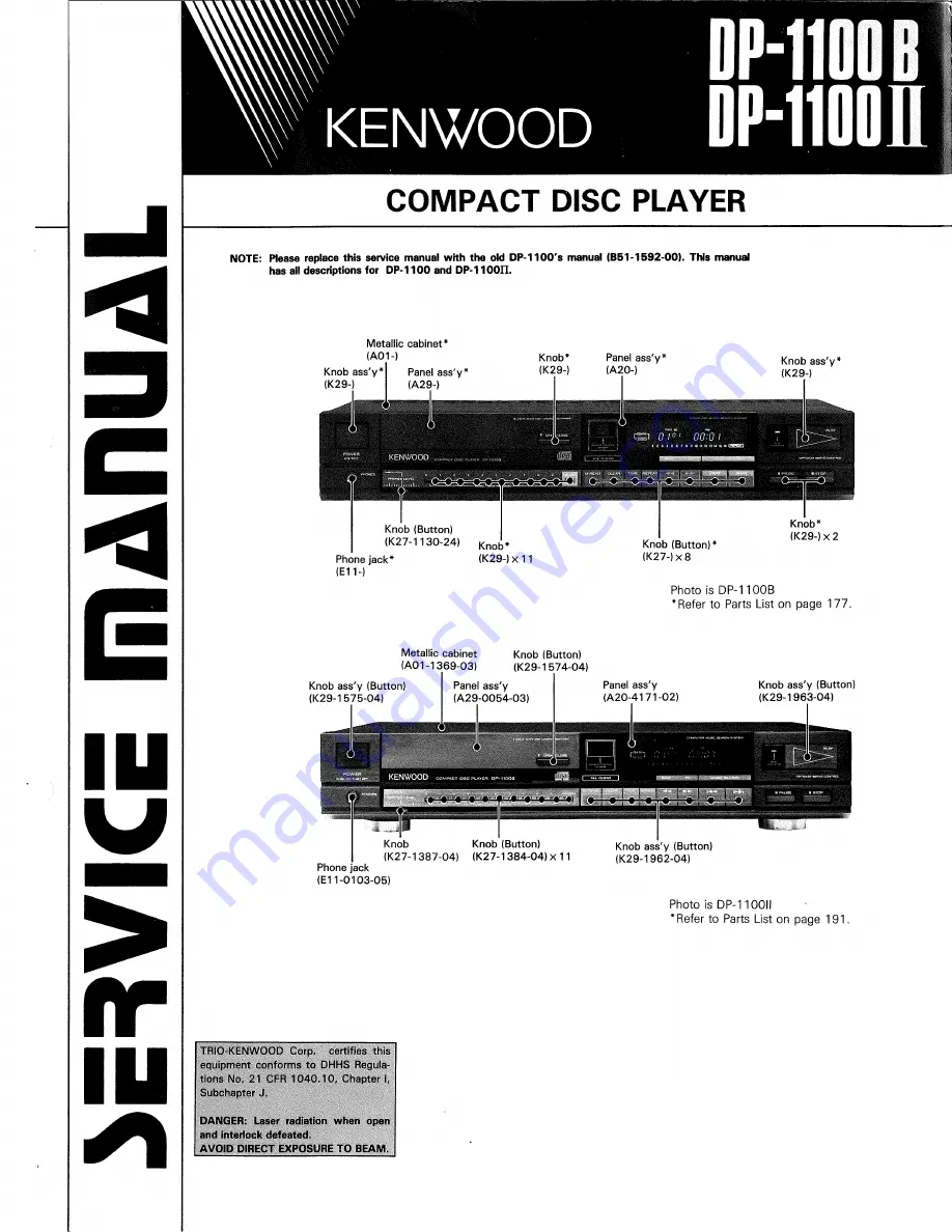
Photo is DP-110011 

'Refer to Parts List on page  1 9 1 , 

TRIO-KENWOOD Corp. certifies this 

equipment conforms to DHHS Regula­

tions No. 21  C F R  1 0 4 0 . 1 0 , Chapter I, 

Subchapter  J . 

DANGER: Laser radiation when open 
and interlock defeated. 

AVOID DIRECT EXPOSURE TO BEAM. 

KENWOOD 

DP-1100 B 

DP-1100II 

Photo is DP-1100B 

•Refer to Parts List on page 177. 

Summary of Contents for DP-1100 B

Page 1: ...or DP 1100 and DP 110011 Photo is DP 110011 Refer to Parts List on page 191 TRIO KENWOOD Corp certifies this equipment conforms to DHHS Regula tions No 21 CFR 1040 10 Chapter I Subchapter J DANGER Laser radiation when open and interlock defeated AVOID DIRECT EXPOSURE TO BEAM KENWOOD DP 1100B DP 1100II Photo is DP 1100B Refer to Parts List on page 177 ...

Page 2: ...FG signal from disc motor FOK Focus servo control signal Servo ON with signal FOK L F O K G Refer to I C 1 5 pin f u n c t i o n on page 6 9 F S R H or F S R C H 2 Hz signal to detect just focusing point It moves the pickup actuator up and d o w n IRQ Interrupt control I O pin between CPU 1 and CPU 2 Interrupt request K G C Inversion signal of signal RFG in IC15 It is normally L and H during kick ...

Page 3: ...D P 1 1 0 0 B II D P 1 1 0 0 B II I BLOCK DIAGRAM ...

Page 4: ... are produced W h e n having transmitted codes described in Fig 1 2 only five codes can be received at the receive side between t t and t5 The number of voltage values reproduced thereby is only five any voltage at timings except t 1 t2 t3 etc cannot be determined However if the frequency component 20 kHz of the original analog signal is less than the value 44 1 kHz depending upon the time interva...

Page 5: ... picking up an analog signal for example 5 0 0 0 0 times per second is called a sampling frequency It is proven that if sampling is conducted at the rate larger than a certain value the original waveform can be reproduced just the same to an inch This is called a sampling t h e o r e m Sampling Theorem If sampling is conducted at the fre quency 44 1 kHz which is over dou ble the maximum frequency ...

Page 6: ...ed a quantization n o i s e The ratio of a quantizing noise against the maximum value of the signal in a binary coded 16 bit system is plotted in respect to a sinusoidal wave input as shown in Fig 1 7 If a 16 bit code is used in quantizing one sampled value the number of steps which can be taken i e the quantizing number N is given as follows W h e n making the amplitude of 0 to V corresponding to...

Page 7: ...als converted into EFM Channel Bits One of 14 bits converted from 8 bits is called a channel bit One word Sample A EFM Symbol 1 17 channel bits Symbol 2 17 channel bits Fig 1 8 1 EFM is the modulation to first divide a 16 bit datum data bit into t w o 8 bit data and then convert each of these 8 bit data to a 14 bit datum channel bit as shown in Fig 1 8 The conversion is to select patterns of 2 8 k...

Page 8: ...0 0 0 1 0 0 0 0 0 1 0 0 0 6 2 0 0 1 1 1 1 1 0 0 0 0 1 0 0 0 0 0 0 1 0 0 0 6 3 0 0 1 1 1 1 1 1 0 0 1 0 0 0 0 0 0 0 1 0 0 0 8 bits 1 4 bits Order data bits channel bits 6 4 0 1 0 0 0 0 0 0 0 1 0 0 1 0 0 0 1 0 0 1 0 0 6 5 0 1 0 0 0 0 0 1 1 0 0 0 0 1 0 0 1 0 0 1 0 0 6 6 0 1 0 0 0 0 1 0 1 0 0 1 0 0 0 0 1 0 0 1 0 0 6 7 0 1 0 0 0 0 1 1 1 0 0 0 1 0 0 0 1 0 0 1 0 0 6 8 0 1 0 0 0 1 0 0 0 1 0 0 0 1 0 0 1 0 0...

Page 9: ...1 1 0 0 0 1 0 0 0 0 0 0 0 0 1 0 0 1 1 8 9 1 0 1 1 1 1 0 1 0 0 0 0 1 0 0 0 0 0 1 0 0 1 1 9 0 1 0 1 1 1 1 1 0 0 0 0 1 0 0 0 0 0 0 1 0 0 1 1 9 1 1 0 1 1 1 1 1 1 0 0 1 0 0 0 0 0 0 0 1 0 0 1 Order 8 bits 14 bits Order data bits channel bits 1 9 2 1 1 0 0 0 0 0 0 0 1 0 0 0 1 0 0 1 0 0 0 0 0 1 9 3 1 1 0 0 0 0 0 1 1 0 0 0 0 1 0 0 0 1 0 0 0 1 1 9 4 1 1 0 0 0 0 1 0 1 0 0 1 0 0 1 0 0 1 0 0 0 0 1 9 5 1 1 0 0 ...

Page 10: ...a m e Frame Sync signals are inserted to indicate the boundary of the frame and to make a bit synchronization Fig 1 9 shows the structure of one frame Channel bits Margin bits Total bits Frame Synchro nization 24 3 27 Users buts 14 3 17 Data bits 14 b i t x 2 4 336 3 b i t x 8 24 72 408 Error correction bits Parity bits 14 b i t x 8 1 1 2 3 bit x 24 136 486 102 588 Frame Structure 1 frame 588 Chan...

Page 11: ... to precautions on handling the disc 7 Playback time is 60 minutes with a 120 m m disc Dimensions are given in Fig 1 12 8 The rotating speed of the disc is not constant Because of a constant linear velocity system employed the rotating speed is varied between around 5 0 0 to 2 0 0 r p m counterclockwise CLV constant linear velocity capstan drive type taperecorder CAV constant angular velocity rim ...

Page 12: ... 0 0 B II Fig 1 12 Lead In TOC table of contents Absolute time of the heading of music is included Lead Out Used for retrieving of the heading indicates of program end Other Control Data P Q 15 Program Lead in T O C Lead out ...

Page 13: ...cess of baseplate Fig 1 16 15 Mastering Procedures for Photo resist coating laser recording and development are included This is corresponding to the fabricating pro cess of a lacquer disc in an analog record production 16 Molding Injection molding Photo Polymerization 6 Disc Surface Disc Baseplate Absorption Reflection attenuation Fig 1 13 PU Objective Lens Dust Pits 1 5 nm j a In a case where du...

Page 14: ...Master Disc Silver Mirror Ni plating Metal Master Ni plating Mother Disc Ni plating Stamper Molding Transparent Disc Finished Good Compact Disc Packing Glass Disc Photoresist Glass Disc Fig 1 16 Manufacturing Process of C D 17 Reflecting Film evaporation Protective file coating Label Printing ...

Page 15: ...ilter Sample Hold ADC Control Display Encoding Error Correction System Sync Generation Modulator Serial Data Output X tal Timing ENCODING SYSTEM time multiplexer Analog to Digital converter Fig 1 17 Encoding system 8 LP Filter Sample Hold ADC Ch 1 MUX MUX ...

Page 16: ... the book if you are reading carefully one character or clause without reading several tens of pages An error collection code is the same as this and correction is easy even w h e n code errors of some bits are present However if many say 1000 bits are consecutively w r o n g at a time it is very difficult to correct those errors Therefore the technique with which an order of a signal is once chan...

Page 17: ...recting method operation of correction is conducted on the assumption that all other data A C and D are correct If there is an error for another article miscorrection happens Bill b A 100 B C 300 D 400 Total P 1 000 Syndrome Checking S A B C D P 0 B B S 200 Disppearance 3 Operating the syndrorme on bill c zero does not come out Therefore it may be found that something is wrong but it cannot be fou...

Page 18: ...A B C D P and Q respectively of bill b for no error EA to EQ 0 k k EAl B B EB C C EC D D E D P P EDl Q Q EQ Obtaining syndrome Sv 5 1 A B C D P A E J B EB C EC D E D P EP A B C D P Ey l E B E c E 0 E F E i 1 0 EA EB EC ED EP Obtaining syndrome S2 5 2 4 A 3B 2C D Q 4A 3B 2C D Q 4E 3 E 2 E C E D E Q 2 0 4 E 4 3 E B 2 E C E D E Q Supposing that a code error is one word between A to P Q I A w r o n g ...

Page 19: ...A B C D P Ey l E f l E c E D E P 2 0 0 0 E B 1 0 0 Supposing EA 0 ED 0 and EP 0 S 1 EJ E C 2 0 0 3 From Equation 2 of 1 S2 4A 3B 2C D 4E 4 3 E B 2 E c E B E Q 500 0 Bill c A 100 B 300 C 400 D 400 P 1 000 Q 2 000 Pointer E c 1 0 0 5 1 A B C D P 200 52 4A 3B 2C D Q 500 Where B E EB C C EC S2 3 E J J 2 E C 5 0 0 4 Determining EB and Ec from simultaneous equations of 3 and 4 This theory is the princip...

Page 20: ... of these words the words passing through No 1 are Q 1 W 1 W 2 W 5 W 8 W 1 5 Q 5 W 5 W 2 W 1 W 4 P U 6 Q 9 W 9 W 6 W 3 W 0 P In other words t w o system of codes are used on both sides of the delay memories Original series of signals W8 W7 W6 W5 p 1 w 1 w 2 w 3 w 4 Qt Wj W2 W_5 W_ W 1 5 PS W5 W6 W7 W8 Q5 W5 W2 W n W_4 P_n Recorded series of signals w5 Qt P 1 5 W_8 W 5 W 2 W t Disc recording sequen...

Page 21: ... I T 3 3 1 Focus Servo Circuit A focus error signal is fed into a focus servo circuit to control a lens system with the use of a focus servo coil like a voice coil of a loudspeaker so that the focus spot of the laser beam is always kept on a pit surface against fluctuations due to the revolutions of a disc The same as auto focusing in an EE camera Disc Lens Signal Processing Focus Servo Focus Coil...

Page 22: ... 3 3 3 4 E Y E P A T T E R N The RF signal is being delivered from the signal processing circuit as described under 3 2 The RF signal is vaired acor ding to appearance or disappearance of a pit on a disc This signal can be displayed on an oscilloscope as illustrated in the Fig 3 5 The waveform is generally called Eye Pattern Fig 3 5 is sketches explaining concept of the eye pattern The RF signal i...

Page 23: ...uniform single wavelength 4 3 P R O P E R T I E S R E Q U I R E D FOR A L A S E R DIODE 1 Oscillation Wavelength According to a CD s proposal there should be the follow ing relaiton between a wavelength of a laser diode and the number of aperture of lens NA X N A 1 7 5 jim As long as today s GaAIAs material is used it is difficult to make a laser diode having a wavelength shorter than apporx 7 6 0...

Page 24: ...ffect of the quarter wave plate the light incoming into the polarizing film is changed so that its polarizing direction is perpendicular to the polarizing direction in the forward path Therefore the light transmits the polariz ing film and does not go back to the semiconductor raSer Next the light incoming into a critical angle prism for detec tion of a foucs point is reflected three times inside ...

Page 25: ...rror must be detected The detection muthods for both errors will be given below 5 2 1 Focus Error Detection W h e n a light beam is passed from a high refraction material to a low refraction material a relaion as shown in Fig 5 2 is existed between the incident angle and refleciton ratio at the boundary of the materials As can be seen from the graphs the reflection ratio will change rapidly as the...

Page 26: ...menon the photo diodes convert light received into four electrical signals and the signals are processed with a differential amplifier to pro vide a focus error signal in terms of At A2 A3 A 4 A1 A 2 A 3 and A 4 Are electrical signals developed by PDa PDb PDc and PDd respectively Critical angle prism Reflection surface Disc too close 4 divided photodiode A3 A 4 Ai A2 A3 A 4 Criticl angle Disc too ...

Page 27: ...g signal in passing through a D A convertor after demodulated 5 4 LIGHT EMISSION F R O M L A S E R DIODE W h e n the LDC goes H the output of T A 7 5 4 5 8 Q 1 0 8 becomes positive as shown in the schematic diagram And a current flowing through R145 D 1 0 2 And D 1 0 4 turns Q109 cut off thereby stops the oscillation of the Laser Diode W h e n the LDC goes to L level the output of T A 7 5 4 5 8 1 ...

Page 28: ...bits is called P Channel Q Channel R Channel W Channel Of the eight channels Q Channel is used for address data and one address data is comprized of 98 frame Q Channel data Fig 5 6 shows this configuration of the CONTROL DISPLAY symbol data Fig 6 1 Frame Syn c h r o n i z a tion Signal Frame Syn c h r o n i z a tion Signal Frame Syn c h r o n i z a tion Signal Frame Syn c h r o n i z a tion Signal...

Page 29: ... Elapsed time minute for each program expressed by BCD in 2 digits 8 bits F R A M E Elapsed time for each program expressed by BCD in 2 digits 8 gits Frame 1 frame 1 75 sec ZERO Not used 8 bits data A MIN Elapsed time sec for disc expressed by BCD in 2 digits 8 bits A S E C Elapsed time sec for a disc expressed by BCD in 2 digits 8 bits A F R A M E Elapsed time for a disc expressed by BCD in 2 dig...

Page 30: ... 1 0 2 The servo control SVC is performed by processor IC12 on the process PCB X 3 2 1 0 1 0 w h e n the disc is exchanged or w h e n play mode is entered from stop mode It checks the number of data errors to control control inputs A B C and INH of Q102 on the mechanism PCB to obtain the optimum playback The internal block diagram and truth table of Q 1 0 2 is shown in Fig 2 1 C and D of section 2...

Page 31: ...10 and Q 1 1 Amplified TE signal drives the pickup actuator coil to form a tracking servo by which the laser beam spot follows exactly the pit sequence on the disc 1 2 3 D S V circuit IC8 1 2 and I C 1 5 D L S 1 and 2 Pits are made on a disc in such a way that the sum of H durations is equal to that of L durations i e DSV Digital Sum Value is zero Thus this circuit controls the amplifier bias so t...

Page 32: ...D P 1 1 0 0 B II 1 CIRCUIT DESCRIPTION Disc Scratch Dust RFES D C O N D O C K Fig 1 2A 3 5 ...

Page 33: ... OFF during play The tracking error TE voltage is amplified to about 6 times in IC14 2 2 and is applied to the bases of Q27 and Q28 through an HPF consisting of C73 and others W h e n the voltage goes up more than about 0 6 V Q27 turns ON while w h e n it goes d o w n less than about 0 6 V Q28 turns ON During that ON period the peak noise of the voltage is suppressed so that the following stage ge...

Page 34: ...e 32 symbol data is corrected for error in the C1 correction section Next after de interleave operation the data which could not be corrected in the C1 correction section is corrected in the C2 correction section Only the data w h i c h could not be corrected even in the C2 correction section is subject to mean value interpolation and is output to the D A converter 1 3 2 C L V servo control in I C...

Page 35: ...represents a sequence of this state 2 Fig 1 4A shows the waveform w h e n signal IOUTR or IOUTL is sampled by signal LRCK W h e n this PAM wave is filtered by an LPF this LPF outputs a music signal with a peak amplitude of 1 2 that of the PAM wave This music signal is input to buffer amplifier IC27 to which a frequency characteristic c o m p e n sotor CR circuit is connected IC26 controls the emph...

Page 36: ...h e n both of pin 14 and 15 are at H level the level of pin 13 changes from H to L The inverted output is obtained at pin 1 1 after going through pin 12 pin 11 is set at L level by R36 but it changes the level from L to H This signal is termed reset signal 5 W h e n the reset signal is H level IC15 T M P 4 7 4 0 N IC12 IC1 and IC15 TC15G008AP 0007 start function ing IC15 TC15G is however reset via...

Page 37: ...of H and L levels at pin 1 to 5 of IC15 TMP4740N as shown below 6 The outputs from pin 1 to 5 of IC15 TMP4740N are applied to pin 24 to 27 and 3 0 and the output is then available at pin 9 of IC15 TC15G or T 7 0 0 1 7 Pin 9 of IC15 TC15G of T 7 0 0 1 has a high impedance for the conditions other than the listed left The input to pin 3 of IC3 is 2 5 V which is obtained by dividing 5 V with R68 and ...

Page 38: ...am a monitor diode provided in the pickup assembly watches the laser emis sion The emission can be held constant by controlling the current through Q 1 0 7 with a help of the monitor diode 5 Q 1 0 6 consists of t w o transistors with the identical characteristics being used under the same conditions same emitter voltage and current Therefore it functions to produce the same base voltage W h e n la...

Page 39: ...aser spot is provided on the disc sur face by moving the pickup lens up and d o w n using the 2 Hz signal This is called focus search operation Once it is focused the search signal is discontinued 4 The output signal from pin 36 of microprocessor IC15 is applied to pin 4 of focus coil drive amp IC2 1 2 via R14 R17 and R18 The focus coil moves the pickup lens up and down Its output appears at pin 2...

Page 40: ...ess than 0 8 V H about 5 V results 2 The time constant for transition to H signal or to L signal is different The time constant for transition to H is determined by C54 and R149 and the time constant for it to L is determined by C54 and R140 The time constant for H is about 1000 times larger than that for L This prevents the output from accidentally becoming H because of dropouts of RF signals cau...

Page 41: ...n 20 Both of the signals are P W M pulse width modulation signals with a carrier frequency of 8 27 kHz in the CLV mode W h e n a disc is revolving at a normal speed both of the AFCO and APCO are clock waveform signals with a frequency of 8 27 kHz at a 5 0 duty Since the AFCO regulates a range of zero revolution to high revolution of the disc motor it may be fixed at H or L level in some in stances...

Page 42: ... of IC1 1 2 through focus gain adjustment trimming potentiometer VR1 and R2 for monitoring gain adjustment 4 Q1 turns ON to inform microprocessor IC15 TMP4740N that a disc has been properly set w h e n the 4 division photodetector detects a reflecting beam from the disc 5 W h e n a reflecting beam from the disc is received pin 2 of comparator IC10 1 2 switches its level from H to L Q31 turns from ...

Page 43: ... TEOP and TEON are added via R167 and R166 and in tegrated in IC12 1 2 The output is used as a TE track ing error signal This output is pulled up by R165 to shift its quiescent point to 0 V so that only an AC component appears 5 The TE signal output to pin 8 of IC14 1 2 is level ad justed and applied to pin 6 of IC1 2 2 The level adjust ment here corresponds to the tracking loop gain adjust ment T...

Page 44: ... 2 is higher than that of pin 3 H level is output to pin 2 W h e n it is lower L level is output 5 Since the input to pin 3 of IC12 2 2 is an inverted input w h e n the input voltage of pin 4 is compared only the dif ference is inverted and made available as an output at pin 2 The output from pin 2 of IC13 112 is applied to pin 2 of IC15 TC15G or T 7 0 0 1 and the output from pin 2 of IC12 2 2 is ...

Page 45: ...pin 8 of IC12 1 2 will be as s h o w n The voltage applied to C70 is 1 5 V 1 5 V 0 6 V 0 6 V in this example The clamper diodes D 2 9 and 31 has no effect to the voltage as shown in the formula because of the directions in which they are put to this cir cuit The voltage applied to C69 is 0 5 V 0 5 V 0 6 V 0 6 V W h e n the pickup is kicked to the selected track and the unit is placed in the PLAY m...

Page 46: ...ignal is applied to pin 7 of IC3 2 2 through R74 Since PLAY is 1 2 V pulled down output of IC16 during normal PLAY m o d e Q 1 4 is OFF In this state IC3 2 2 and RC components form a low pass filter As a result the high frequency components are eliminated from T C O signal to obtain offset signal It is applied to pin 3 of IC4 2 2 through R78 After gain adjusted it drives the pickup carry motor thr...

Page 47: ...unction of Q6 and Q2 controls the opera tion of focus coil It is disabled by this circuit w h e n no focusing is required 2 W H E N A D I S C IS L O A D E D A N D IN P L A Y MODE 1 W h e n a disc is loaded a signal picked up by the 4 division photodetector is divided into t w o signals Si and S2 by Q103 TA7331P They are amplified by Q21 and fed to pin 3 of IC10 1 2 2 W h e n the RF signal is prese...

Page 48: ...ut detec tion signal of L level is provided at pin 12 DCON of IC15 at the same spot per every revolution of the disc The signal is applied to pin 2 of IC16 It is level shifted and its inverted output is available at pin 14 The signal is fed to the base of Q8 and to the gate of Q9 in order to reduce the gain of Q8 and also to vary the phase compensation of Q9 so that the pickup does not j u m p fro...

Page 49: ...a feedback terminal R121 is a feedback resistor to determine the output level at pin 1 of A B signal W h e n one of R107 through R111 is con nected in parallel the ouptut level varies R119 and R120 are feedback resistors to determine the ouptut level pin 16 of the C D signal and R120 is a trimming poten tiometer to adjust the initial condition of SVC 5 The A B signal and the C D signal are applied...

Page 50: ...is pro tected against scratches or shocks 2 If a scratch is found on the surface of a disc pin 8 RFES of comparator IC10 2 2 is switched from L level to H level and pin 22 of IC15 turns to H level W h e n pin 22 becomes H level a shift register is set inside IC15 and the DOCK signal 120 pulses per one revolution of disc is counted Both of the shift register inside IC15 and external register IC9 ar...

Page 51: ...pin 4 of IC11 1 2 is set at 2 5 V by R157 and R156 the output from pin 2 of IC11 1 2 becomes 0 V 4 PUFF available t pin 33 of IC15 is also high impedance during the normal PLAY mode The input at pin 7 of IC11 2 2 becomes 2 5 V by R160 and R162 Since the input voltage at pin 6 of IC11 2 2 is set at 2 5 V the output at pin 8 becomes 0 V 5 W h e n the pickup is moved in the FORWARD FF direc tion PUFF...

Page 52: ...the same time Pin 26 to 29 are input lines and they are all 0 V when no keys are pressed For example w h e n the PLAY key is pressed The pin 14 line and pin 26 are shorted and scanning pulse from pin 14 is input to pin 2 6 IC1 4 bit microprocessor recognizes that the PLAY key has been pressed based on the input to pin 26 and the timing of pulse at pin 14 and gives the PLAY instruction to IC15 cont...

Page 53: ...todetector is shaped into a proper waveform converted to a TTL level and fed to pin 17 EFMI of IC15 as EFM signal 2 The EFM signal input to pin 17 of IC15 goes through a buffer and EFMO signal is output to pin 4 1 It is then ap plied to pin 14 of IC9 Being locked by bit lock signal PLCK DOUT signal with its jitter component eliminated is produced Refer to section 1 5 18 PLL CIRCUIT OPERA TION The ...

Page 54: ...g the SEARCH m o d e however the reference voltage is raised up about 3 V to shorten the search period For this purpose an RFG signal of L level is ap plied to the base of Q15 to turn it ON and its H output is added to I N A through R110 during the SEARCH period 4 The output from pin 4 OUTA of low pass filter output controls voltage for VCO through R15 The VCO has been designed to oscillate at abo...

Page 55: ...on the former is called analog muting and the latter is called digital muting 2 Pin 38 of IC15 TC15G or T 7 0 0 1 is at L level during all modes except normal PLAY mode and it provides 0 V to the base of Q4 Q4 is turned OFF making relay RL1 OFF The output is thus muted At the same time pin 3 4 of IC6 TC9179F is also held at L level through R103 The output of 16 bit digital signal is turned OFF ins...

Page 56: ...h the input signal The quies cent point current is determined by load resistor R29 and B supply The varying current signal is fed to pin 7 of remoto control a m p IC17 It is about 4 0 dB amplified here and the output is available at pin 1 2 The signal is fed again to pin 2 of IC16 through the detec tion circuit of D 1 4 amplification centering around 3 8 kHz The output appears at pin 7 The signal ...

Page 57: ...een emphasized its information has been included in the subcode data of the disc To lower the high frequency level during PLAY mode is called de emphasis PROCESS IC8 TC9178F outputs pin H level at pin 12 by reproducing and decoding EFM signal if the playing disc is an emphasized one The signal is sent to the base of Q6 R220 C 2 2 8 R 2 2 1 C 2 2 9 are high frequency damper elements W h e n Q6 turn...

Page 58: ...IT AND PIN DESCRIPTION 2 1 Head amp J25 4404 08 2 1 1 Q 1 0 3 T A 7 7 3 1 P head amp Q103 TA7731P is the head amp and operation IC for the laser beam receiver device developed for CD system DAD player Pin connection diagram 61 Block diagram ...

Page 59: ...division photodetector outputs Note 1 5 IN B Input pin of signal B one of 4 division photodetector outputs Note 1 6 IN C Input pin of signal C one of 4 division photodetector outputs Note 1 7 IN D Input pin of signal D one of 4 division photodetector outputs Note 1 8 GND1 GND pin 9 10 NC Not connected 11 Positive supply voltage pin 12 0UT4 Pin which outputs the sum signal B D of pin IN B and IN D ...

Page 60: ... signals out of 4 division photodetector outputs The final stage buffer amp is provided with an external feedback resistance to neutralize the effect of the irregularity in characteristics between photodiodes J J k RF2 J T OUT 2 fa Buffer amp Note 1 With max input of 100 kHz Transfer impedance 27 kfi Rn 9k0 Table 2 1A Note 1 4 division photodetector configuration 6 3 ...

Page 61: ...tiplexer capable of selecting analog or digital signal or combining them The switch pin corresponding to each channel turns ON with the digital signal from the control pin Truth table Block diagram CONTROL INPUTS O N CHANNEL INHIBIT C B A TC4051BP L L L L 0 L L L H 1 L L H L 2 L L H H 3 L H L L 4 L H L H 5 L H H L 6 L H H H 7 Fig 2 1D Table 2 1 C 6 4 ...

Page 62: ...2 2 Servo board X29 1520 00 2 2 1 I C 9 T C 5 0 5 0 P dropout memory 50 stage 114 stage selection type shift register Pin connection diagram Block diagram Logic diagram Truth table t t n tn 50 tn 64 IM OM Dot r OM Dour H H L H H H L H L L H L H L L H H H L L L L H L 6 5 ...

Page 63: ...D P 1 1 0 0 B II 2 IC OPERATION OF EACH CIRCUIT AND PIN DESCRIPTION Fig 2 2 2 A 6 6 2 2 2 I C 1 5 T C 1 5 G 0 0 8 A P semi custom IC Pin connection ...

Page 64: ...D P 1 1 0 0 B II 2 IC OPERATION OF EACH CIRCUIT AND PIN DESCRIPTION Block diagram Fig 2 2 2 B Internal block diagram 6 7 ...

Page 65: ...orated 6 TEG1 Tracking error detector control 2 input I L L Stop of tracking error detection TEOP is fixed to L TEON is fixed to H Pullup resistor incorporated 6 TEG1 Tracking error detector control 2 input I Pullup resistor incorporated 3 TEON Tracking error negative output 0 When TS2 advances in edge phase against TS1 outputs a L signal at normal operation 4 TEOP Tracking error positive output 0...

Page 66: ...the RF signal regenerated by the PU through a comparator Its polarity should be positive against the RF signal polarity Pullup resistor incorporated 18 TS2 Tracking error generation signal 1 input I Input for binary signal obtained from passing the A2 A4 signal of 4 division photodetector through zero cross comparator Used in tracking error generation Pullup resistor incorporated 19 TS1 Tracking e...

Page 67: ...l at an optimum level 30 MODE 0 Mode select signal input I Input for servo system control signal generation and kick operation pro cess direction indication Connected to the microprocessor Pullup resistor incorporated 31 TEST Test I Normally open or connected to VD D Pullup resistor incorporated 32 PUFF PU motor fast carry signal output 0 H output FWD L output BWD HiZ OFF 3 state output 33 KICF PU...

Page 68: ...FG signal with 20 pulse disc rotation Should have a duty ratio of approx 50 Pullup resistor incorporated 40 PLCK PLL section clock pulse input I Input for reference signal 4 32 MHz to PLL section for EFM signal reading Pullup resistor incorporated 41 EFMO EFM output 0 Inversion output of signal EFMI With signal RFOK H is fixed to L 42 5 V Table 2 2 A 71 ...

Page 69: ...0 0 HiZ BWD search Stop BWD mode 0 0 0 0 8 0 0 0 1 0 0 HiZ 1 Tray close laser diode ON 1 0 0 1 0 9 1 1 1 1 1 0 0 HiZ PU motor kick before BWD search 0 1 0 0 A 1 1 1 1 1 D 6 HiZ Play mode 2 4 1 1 0 0 B 1 1 1 1 1 0 1 HiZ PU motor kick in FWD search 0 0 1 0 C 0 0 0 0 0 0 HiZ 1 Tray close laser diode OFF 1 0 1 1 0 D 0 0 0 0 0 0 0 HiZ Eject BWD mode 0 1 1 0 E 0 0 0 0 0 0 HiZ 0 Tray open Open from ON of...

Page 70: ...t 0 1 0 0 2 BWD1 TRACK KICK 1 1 0 0 3 FWD1 TRACK KICK 0 0 1 0 4 BWD3 TRACK KICK 1 0 1 0 5 FWD3 TRACK KICK 0 1 1 0 6 BWD5 TRACK KICK 1 1 1 0 7 FWD5 TRACK KICK 0 0 0 1 8 BWD7 TRACK KICK 1 0 0 1 9 FWD7 TRACK KICK 0 1 0 1 A BWD15 TRACK KICK 1 1 0 1 B FWD15 TRACK KICK 0 0 1 1 C BWD31 TRACK KICK 1 0 1 1 D FWD31 TRACK KICK 0 1 1 1 E BWD CONTINUOUS Kick 1 1 0 0 F FWD CONTINUOUS Kick Table 2 2 C T C 1 5 G ...

Page 71: ...D H 1 0 0 B II 2 IC OPERATION OF EACH CIRCUIT AND PIN DESCRIPTION 2 3 Process board X32 1010 00 2 3 1 I C 1 5 T M P 4 7 4 0 N 5 9 0 9 5 9 1 4 Main microprocessor 7 4 Fig 2 3 1A ...

Page 72: ... to the external RAM IC14 TC 5514P 9 R6 R60 AO 0 H Address data output to the external RAM IC14 TC 5514P 10 R6 R61 A3 0 H Address data output to the external RAM IC14 TC 5514P 11 R6 R62 A4 0 H Address data output to the external RAM IC14 TC 5514P 12 R6 R63 A5 0 H Address data output to the external RAM IC14 TC 5514P 13 R7 R70 DO QDAd I O H 1 Data input terminal of the subcode Q from IC8 TC 9178 T ...

Page 73: ...L level with the tray opened 2 Disc existence judge signal L level when a disc exists 28 KO K02 SLT I Pickup position detect signal input H level when the pickup is positioned in the program area and L level in the read in area 29 KO K03 RFOK I RF signal input L level when RF signal exists 35 R8 R80 IRQ I O H Data transfer request signal from IC1 TMP47C41N Usually H level and goes to L level when ...

Page 74: ...OOB n 2 IC OPERATION OF EACH CIRCUIT AND PIN DESCRIPTION Pin No Port name Signal name IN OUT Level Function operation 34 Power supply Power supply 5 V 42 v D D Power supply Power supply 5 V Table 2 3 1 A 77 ...

Page 75: ...tive LPF and a data separation circuit The digital phase comparator detects the phase error bet w e e n the clock pulse obtained from 4 division of the VCO output and the reference of the HF signal EFMI emitted from the data slicer Then from the charge pump circuit up and d o w n signals UO and DO are output as phase error data Pin connection diagram Block diagram Fig 2 3 2 A 7 8 Fig 2 3 2B T D 6 ...

Page 76: ...ency is phase delayed in rising edge against signal EFMI input its L output duration is prolonged to make VCO fre quency higher In phase lock L level 1 2 PLCK High impedance state ex cept during L direction 8 DO Charge pump down signal output pin When signal PLCK obtained from 4 division of VCO frequency is phase advanced in rising edge against signal EFMI input its H output dura tion is prolonged...

Page 77: ...utput synchronized with the rising edge of signal PLCK is input to pin EFMI of C MOS processor TC9178F C MOS level 14 EFMI Input for EFMI signal obtained by passing the RF signal regenerated from disc through data sheer TTL level 15 Voce Voltage supply to digital circuit 16 Positive voltage supply pin to analog circuit Table 2 3 2 A 80 ...

Page 78: ...D P 1 1 0 0 B II 2 IC OPERATION OF EACH CIRCUIT AND PIN DESCRIPTION 2 3 3 IC8 T C 9 1 7 8 F E F M decoder Pin Description Pin connection Fig 2 3 3 A 81 ...

Page 79: ...D P 1 1 0 0 B II 2 IC OPERATION OF EACH CIRCUIT AND PIN DESCRIPTION T C 9 1 7 8 F Block diagram Fig 2 3 3 B 8 2 ...

Page 80: ...Connected to each of TC9179F DIV pin 65 and D I V pin 64 5 D I V I Appears only at high disc rotation L L 1 288 Connected to each of TC9179F DIV pin 65 and D I V pin 64 5 D I V I Appears only at high disc rotation H L L 1 287 5 Higher Connected to each of TC9179F DIV pin 65 and D I V pin 64 5 D I V I Appears only at high disc rotation H L H 1 287 Higher Connected to each of TC9179F DIV pin 65 and ...

Page 81: ... I FG IN pulse setting Either of 1 or 4 pulse per each rotation can be set 15 4 1 I 4 1 FG pulse per each disc motor rotation 15 4 1 I H level 1 15 4 1 I L level 4 15 4 1 I 16 OVRG I At start On play CLV appl 5 V 0 V r cation begins Pin to select whether or not disc motor rotation control is performed by FG IN input H FG IN input valid 17 APCG I H ON OFF selection input of APC signal generator for...

Page 82: ...4 outputs of sub code signal SCT T S W 22 SCSE I L level Data of 4 bits P Q R and S is output 22 SCSE I H level Data of 4 bits T U V and W is output 23 26 SC P T SC Q U SC R V SC S W 0 8 bit data output of sub code signal P Q R S T U V W This signal is the data of each frame Here 4 bit data is output by signal SCSE as required Data selection of each frame is performed in syn chronization with the ...

Page 83: ...t data reading is disabled ZTJ__ p 5 V Li J J 5 M S j EE M3 mS j 5 V 5 mV V 1 y o v 13 mS QDAS _ n _ n With block error Data selection input for sub code signal Q data outputs QAD a to QAD d For easier interface with the microprocessor this input deter mines output data at QDA a to b QDRE and QDE ports 37 QDAS I D A T QDAa QDAb QDAc QDAd L QDRE QDEa QDEb L H QDAa QDAb QDAc QDAd 34 35 NC Not connec...

Page 84: ...h is input from pin EFM2 43 TMWS 1 TMWS N PLCK 43 TMWS 1 L 11 1 43 TMWS 1 H 11 0 5 43 TMWS 1 44 FSGM 1 When no frame sync pattern is detected within the window of the frame sync separation protection gate signal in N continuous frames system synchronization is made by the next input frame sync pattern without the window These two inputs are used in selection of number N 44 FSGM 1 FSGL FSGM N frame...

Page 85: ...es output TMO into high impedance state Normally it is connected to FSPS or FSLO 51 FSPS 0 This appears when no synchronization is obtained over some frames N 20 mS Output to indicate the system sync state on the frame sync pattern Becomes H when no sync pattern is given within the window of gate signal in N continuous frames on selection by input FSGL or FSGM 52 EFM2 I j o 2 M S Input of EFM sign...

Page 86: ...puts When pin BOEN is L data is output DBOO LSB to DB07 MSB Note Connected to I O 0 7 p i n s 1 9 2 6 of TC9179F IC6 5 7 6 0 6 2 6 5 DBOO DB07 0 Outputs for demodulation data U0 to U 3 1 in each frame These are 3 state outputs When pin BOEN is L data is output DBOO LSB to DB07 MSB Note Connected to I O 0 7 p i n s 1 9 2 6 of TC9179F IC6 66 BOEN I I j i f 3 8 tS Input for enable signal which turns ...

Page 87: ...D P 1 1 0 0 B II 2 IC OPERATION OF EACH CIRCUIT AND PIN DESCRIPTION 2 3 4 IC6 T C 9 1 7 9 F Error correction Pin connection Fig 2 3 4 A 9 0 ...

Page 88: ...D P 1 1 0 0 B II 2 IC OPERATION OF EACH CIRCUIT AND PIN DESCRIPTION Block diagram Fig 2 3 4 B T C 9 1 7 9 F Block diagram 91 ...

Page 89: ...ternal RAM address data output Connected to address data input of external RAM 5 1 4 18 AD0 AD9 AD10 0 1 0 M S 5 V 0 2 OV External RAM address data output Connected to address data input of external RAM 15 R W 0 ft 3 4 nS Read write signal output to external RAM Connected to R W input of external RAM L Read H Write 16 CE2 0 Chip enable 2 signal is output when external RAM is read or written Connec...

Page 90: ...n amount decreases it shifts to 0 dB side 35 MUT 01 0 Muting 1 output Outputs an L signal when burst error over 64 frames or buffer over of jitter absorption memory is detected 36 MUT 02 0 Muting 2 output Outputs an L signal when deinterleave error is detected over 3 continuous frames 37 I C utput data parallel serial selection input 37 P S SE I C L parallel output H serial output 38 DA 0 0 Not co...

Page 91: ... LSB of 8 bit data APL output Outputs R channel aperture signal Not connected 45 DA 5 0 Not connected 46 DA 6 0 Not connected 46 DA 6 0 P S SE L P S SE H Not connected 46 DA 6 0 Outputs the seventh bit from LSB of 8 bit data APL output Outputs L channel aperture signal Not connected 46 DA 6 0 Not connected 47 DA 7 0 T T T V V 47 DA 7 0 T T T V V P S SE L P S SE H 47 DA 7 0 Outputs MSB of 8 bit dat...

Page 92: ...al required in the system Feedback resistance and amp incorporated X tal OSC frequency 8 4672 MHz 53 X 1 I ALALy o v 0 05 tiS X tal OSC connection pins X tal OSC is connected to generate the clock signal required in the system Feedback resistance and amp incorporated X tal OSC frequency 8 4672 MHz 54 CKSE I Selection pin which informs X tal OSC frequency Pullup resistance incorporated H or open 8 ...

Page 93: ... 4 frames This output is connected to pin DIV of TC9178F IC8 to lower the disc motor revolution Connected to DIV pin 5 of TC9178F IC8 65 DIV 0 138 nS Buffer memory status output Outputs an H signal when the jitter absorption buffer memory enters range of 2 or 3 frames in its capacity of 4 frames This output is connected to pin DIV of TC9178F IC8 to raise the disc motor revolution Connected to DIV ...

Page 94: ...DP 1100B II 2 IC OPERATION OF EACH CIRCUIT AND PIN DESCRIPTION 2 3 5 I C 1 2 M B 8 8 2 0 1 1 1 5 K S V C mircoprocessor Pin connection diagram Fig 2 3 5 A Block diagram Fig 2 3 5B 9 7 ...

Page 95: ...rors halts request signal When track jump occurs becomes H After that stops operation for 1 2 msec 1 R6 CIER I 1 Input for block error signal from IC11 When block error occurs becomes H 2 R7 COFS I 1 Input for corrected frame period signal 7 35 kHz square wave from IC6 At the point when it becomes H signal CIER is judged 3 R8 EOF 0 1 Output for focus offset amount control data to Q102 TC4051BP Not...

Page 96: ...l 3 From the level of which the count exceeded 2 0 0 0 the offset level is stepped up 3 levels in this case to level 6 N B for enough clearance margin for block error numbers This level is main tained till the end of playback unless the disc is changed or stopped For counting of the number of block errors the number of times by which block error signal CIER from IC11 TC4094BP generated in synchron...

Page 97: ...D P 1 1 0 0 B II 2 IC OPERATION OF EACH CIRCUIT AND PIN DESCRIPTION 2 3 6 I C 1 4 T C 5 5 1 4 P T O C Memory Pin connection diagram Fig 2 3 6 A 1 0 0 ...

Page 98: ... each preset channel 4 Area of total play time of each channel First the method of access to the area of read in data Area 1 is described As shown in Table 2 3 6A IC14 is so configured that row address is designated by microprocessor ports R52 and R53 LSB data of column address by 4 ports R6 and MSB data of column address by 4 ports P 1 Here the microprocessor is programmed so that the binary conv...

Page 99: ... DATA CH TIME TOTAL TIME 8 2 TNO L 1 MIN 1 MIN Unused CH1 CH DATA CH TIME TOTAL TIME 8 3 TNO H 10 MIN 10 MIN Unused CH1 CH DATA CH TIME TOTAL TIME 8 4 Unused 100 MIN Unused CH1 CH DATA CH TIME TOTAL TIME 8 5 Unused Unused Unused CH1 CH DATA CH TIME TOTAL TIME 8 6 Unused Unused Unused CH1 CH DATA CH TIME TOTAL TIME 8 7 Unused Unused Unused CH1 CH DATA CH TIME TOTAL TIME 8 8 INDEX L 1 SEC 1 SEC Unus...

Page 100: ... min 41 s e c is written on the point data of tune 2 0 which is read out in reading the read in data Fig 2 3 6B As mentioned above the binary conversion data of the point data read out is used as column address Therefore in this case tune 20 the column address is H 14 Data is written or read in order from sec digit 1 0 3 ...

Page 101: ... T h e head column address for each channel is represented by a hexadecimal number For this purpose the result of subtraction by 1 from channel data CH 1 to CH 16 is con verted to a hexadecimal number to which H 80 is then add ed Thus the result of this addition is used as this head col u m n address In this case CH 16 therefore the head col umn address is H F8 0 4 ...

Page 102: ...D P 1 1 0 0 I I 2 IC OPERATION OF EACH CIRCUIT AND PIN DESCRIPTION 2 3 7 IC26 PD4053BC Pin connection Fig 2 3 7 A Block diagram Fig 2 3 7B 1 0 5 ...

Page 103: ...s turned off Not an emphasized Q6 is turned on Control inputs O N Channel INHIBIT C B A O N Channel L L L L Z0 Y0 X0 L L L H Z0 Y0 Xt L L H L Z0 Yi X0 L L H H Z0 Yi Xj L H L L Zi Y0 X0 L H L H Zi Y0 Xx L H H L Zi Yi X0 L H H H z Yi Xx H X X X NONE H High level L Low level X H or L Table 2 3 7 106 ...

Page 104: ...D P 1 1 0 0 B II 2 IC OPERATION OF EACH CIRCUIT AND PIN DESCRIPTION 2 4 Display PC board X25 2020 00 2 4 1 IC1 T M P 4 7 C 4 1 N display microprocessor Pin connection diagram Fig 2 4 1 A l ...

Page 105: ...e data Grid Bit 2 10 R6 R61 FD3 0 0 FL display tube data Grid Bit 3 11 R6 R62 FD4 0 0 FL display tube data Grid Bit 4 12 R6 R63 FD5 0 0 FL display tube data Grid Bit 5 13 R7 R70 FD6 0 0 FL display tube data Grid Bit 6 14 R7 R71 FD7 0 0 FL display tube data Grid Bit 7 15 R7 R72 FD8 0 0 FL display tube data Grid Bit 8 17 R7 R73 FD9 0 0 FL display tube data Grid Bit 9 17 P1 P10 FSA 0 FL display tube ...

Page 106: ... remote control signal This signal is input in the PPM system using NEC remote control IC tPD1943G Reception processing is made in its reading edge 38 R8 R83 TP I O 1 TP in ut n p U t t i m e r p a y s e l e c t o n signal input H timer play function turns OFF 38 R8 R83 TP I O 1 CHIRP output Output for chirp sound control signal Not connected Becomes H for approx 0 072 sec after pressing the key 3...

Page 107: ...respond to anode segments a to k of FL display tube and pins FD1 to FD9 to the grid pins of the respective display digits For key scan 1 0 3 3 6 Hz obtained from 4096 division of the reference clock signal frequency 4 2 3 3 6 MHz is used as the scan frequency The system in w h i c h scan is made to grid G9 alone twice in one cycle is employed because of wide display area etc Accordingly scan to to...

Page 108: ...2 IC OPERATION OF EACH CIRCUIT AND PIN DESCRIPTION o 968msec Fig 2 4 1 B Timing diagram for each segment and digit 11 Fig 2 4 1B Display matrix in FL tube display section ...

Page 109: ...O X MIN and SEC in order However when the tray is opened all digits go off In addition when a numeral key or the M READ key is operated TNO and X X may not be displayed alone are displayed and MIN and SEC are blanked Then during search TNO and X X may not be displayed blink and MIN and SEC go off The display for mat is shown below O N i C J C C Z 77 O C D U L J l __ _D O _ C D _D 0 1 2 3 4 5 6 7 8...

Page 110: ...0 0 0 1 0 K03 KS 3 29 0 0 0 1 0 0 0 1 0 0 0 1 Accept key 0 1 2 3 4 5 6 7 8 9 TIME OPEN CLOSE Digit FD 7 R71 FD 8 R72 FD 9 R73 Port name Signal name Pin No 14 15 16 KOO KS 0 26 1 0 0 0 1 0 0 0 1 0 0 1 K 0 K01 KS 1 27 0 1 0 0 0 1 0 0 0 1 0 0 K 0 K02 KS 2 28 0 0 1 0 0 0 1 0 0 0 0 0 K03 KS 3 29 0 0 0 1 0 0 0 1 0 0 1 1 Accept key PLAY PAUSE STOP REPEAT FF REV UP DOWN CLEAR ME MORY M READ ALL CLEAR Fig ...

Page 111: ...re distinguished by periodical length shown in Fig 2 4 1G In addition w h e n a key is pressed con tinuously the output after 108 msec does not become the same code as before Thus leader codes alone each with 9 msec L period and 2 25 msec H period appear con tinuously In this system the falling edge of the reception signal is detected by interrupt function INT1 of IC1 TMP47C41N and then the time t...

Page 112: ...2 IC OPERATION OF EACH CIRCUIT AND D P 1 1 0 0 B II PIN DESCRIPTION Fig 2 4 1 G 1 ...

Page 113: ...les The following describes the main ones 3 1 1 Tray close operation The microprocessor sends a mechanism control instruction to servo PCB IC15 TC15G and performs this operation while monitoring the mechanism condition by switches Fig 3 1A shows the operation flow chart Fig 3 1 A Operation flow chart ...

Page 114: ... the operation flow chart Words at the left of pin DOK of CN2 becomes L so this detection can be made some steps denote pin names of IC15 The pickup lens is moved forwards and backwards by signal FSRCH 2 5 Hz to search for the focusing point Thus w h e n pin DOK does not become L even after 2 cycles of this signal the microprocessor judges that no disc is present Fig 3 1B Operation flow chart 18 ...

Page 115: ...ved backwards about 2 3 m m from this point to the center of the disc lead in area by backward kick operation and lead in data reading starts W h e n reading cannot be completed even after approx 2 0 sec reading is stopped and operation shifts to search opera tion of the first tune In this case dynamic search and c o m p u tation of various times performed based on TOC data become impossible Fig 3...

Page 116: ...ttern 4 bit control data Selection of 2CH 4CH play signals Designates pre emphasis ON OFF and digital copy enable disable ADR 4 bit mode data MODE 1 BCD 1 Address mode MODE 2 BCD 2 Disc catalog number mode MODE 3 BCD 3 Special information mode Written by 0 to 9 and A to Z alphanumeric characters MNR Music number expressed by 2 digit BCD 8 bits X Index in each music expressed by 2 digit BCD 8 bits ...

Page 117: ...DP 1100B II I OPERATION OF MAIN MICROPROCESSOR Fig 3 1D Q data reading flow chart ...

Page 118: ...uting is released until the next kick operation starts In this way operability is improved with w h a t is called cue review operation In simple key pressing of less than 0 5 sec and continuous forward backward feed operation in play mode the pickup feed speed is almost constant even w h e n the FF REV key is pressed in any pickup position on the disc by use of the method described in the followin...

Page 119: ... external RAM IC14 TC5514P the play start absolute time of each tune record ed in the disc is stored Thus in the dynamic search system the time difference between the absolute address of the searching program read out from the external R A M and the present absolute address is converted to the difference in number of tracks by the conversion table and at the same time the ripple of the RF signal g...

Page 120: ...he disc edge FWD search mode Code 7 is output to semi custom IC15 T7001 0 0 0 7 or TC15G0008AP to turn ON the pickup motor Then FWD continuous kick mode Code F K I C K is output to start kick operation 7 2 W h e n AT is a minus number i e w h e n search is per formed in the direction of the disc center BWD search mode Code 6 is output and then BWD continuous kick mode Code E K I C K is output to s...

Page 121: ...D P 1 1 0 Q B II OPERATION OF MAIN MICROPROCESSOR Fig 3 1 E Operation flow chart of dynamic search system ...

Page 122: ...on is executed In addition w h e n TOC data is not read out dynamic search operation cannot be performed In this case therefore all search operation is performed in the kick search system Against this case in DP 1100B II a self learning function of TOC data is produced by writing in external RAM the absolute time on completion of search operation so that the subse quent search operation can be per...

Page 123: ...time difference 2 W h e n the searching position is outside the present posi tion forward kick operation in which the pickup is moved by the number of tracks corresponding to the stage No is performed W h e n the searching position is inside backward kick operation in which the pickup is moved by the number of tracks corresponding to the stage No is performed 3 After completion of kick operation t...

Page 124: ... is nearly doubled is taken to shorten the search time 5 Process advances to step 6 or 7 according to whether or not backward 1 track kick operation is made 6 The stage No is lowered by 1 to reverse the kick direc tion However as shown in Table 3 1D if the last pickup movement was the forward 1 track kick backward 1 track kick operation is further made until the pickup crosses the searching positi...

Page 125: ...to improve precision in pause operation 2 The stage No in which kick starts is set to stage 2 backward 3 track kick upon which search operation is then started 3 Even w h e n search is converted kick in the direction of the disc center is performed to continue search opera tion 4 W h e n the key operation to cancel pause mode is per formed the pause operation search operation is c o m pleted after...

Page 126: ...4 After transmission of the transmission completion data pin DAT21 is returned to L and transmission is c o m pleted b Data transmission from IC1 T M P 4 7 C 4 1 N to I C 1 5 TMP4740N 1 The data to be t r a n s m i t t e d is p r e p a r e d IC1 TMP47C41N 2 Pin IRQ is made L IC1 TMP47C41N 3 4 bits of transfer clock pulses SCK are output IC15 TMP4740N 4 4 bit data is received IC15 TMP4740N 5 For re...

Page 127: ...2 s e c Focus error DOK Focus servo When there is no disc the laser diode goes out then focus search stops and fluorescent indication D I S C goes out DISC motor start RFOK is detected Focus servo on Focus search stop Tracking servo on IC15 MSP A F C CLV S1 S2 EFM RFOK Focus servo AGC Slice level FOK T max is detected Focus servo FOKG KGC TE Tracking error Tracking servo Dropout control Rising edg...

Page 128: ... 00 Is indication normal Display circuit Press the PLAY button Is sound heard Is it free from abnormal sound Signal processing DAC Is there sound skipping Tracking servo dropout control Is the time indication advanced Display circuit main microprocessor Press the PAUSE button 3 I Is the sound muted Signal processing DAC IC19 Is the time indication stopped at a certain reading Kick circuit r Press ...

Page 129: ... FF BWD Is the above operation normal Kick circuit display circuit 1 Press the STOP button Does the disc stop rotating in 10 seconds during the pause of the first program Display circuit main microprocessor Press the tray switch E J E C T i Does the disc motor stop and the tray comes out Main microprocessor tray circuit Operation ok ...

Page 130: ... until search for the first program is completed M PLAY Lights in memory play mode M SCAN Lights when the M SCAN function is ON TOTAL TIME Lights when the time display mode is the absolute time mode TOTAL REMAINING TIME Lights when the time display mode is the remaining time mode REMAINING REPEAT Lights when the repeat function is ON MEMORY CHANNEL In manual play mode those lamps corresponding to ...

Page 131: ...d upwards and d o w n w a r d s a t 1 m m Y E S Check the RF amp Check the slice level control Check the AGC R24 1 2 0 0 outputs Y E S Check the AGC amp Is the RF amp ok Check the slice level control Check the comparator Y E S Is a minus signal applied to the base of transistor and the gate of the FET in the FOK cirucit Q2 and Q6 N O Y E S Check the resistor array and the conductor pattern foil 1 ...

Page 132: ...eck the limiter amp Q27 Q28 Q30 and IC14 Confirm by using a disc relatively free from scratches C K 8 8 8 8 2 k H z ICI 5 5 iS The a c t u a t o r a n d the parts associated with the pickup are defective FOKG Is the RFOK signal fed to the microprocessor F o r KGC and D C O N refer to respective chapters N O Check the tracking error amps I C I IC2 Q 1 1 Q10 D10 and D 1 1 Are TS1 and TS2 output norm...

Page 133: ...in operation While the BWD is in operation While the FF is in operation YES N O r Check the semi custom IC Check the TES IC13 2 2 Check RFES IC10 2 2 Check the inverter buffer IC16 Ser vo PCB Check the microprocessor mode Note Note Unless the TES and RFES are in operation search is not possi ble beacuse TTAC is not output If the tracking gain increases too much the actuator sound becomes conspicuo...

Page 134: ...k detection amp IC8 for AGC Check the Q33 Check the remote control circuit Check the microprocessor mode Refer to the description of IC15 the state of mode 0 to 4 4 9 SLICE LEVEL CONTROL D S V The slice level con trol is not effective YES Check the auto slice level control amp IC8 pins 28 and 29 of IC15 Servo PCB Note The AGC circuit makes the input level to the RF amp constant when the input leve...

Page 135: ...heck the delay circuit in the stop mode R217 R218 and C76 Note When there are too many scrat N O ches the signal t e n d s to go high Is PLCK 4 3 MHz Q I 4 Emitter 4 3 M H z CN11 p i n 3 These appear w h e n the same frames are not in sync pin 3 of C N 1 1 1 7 0 Hz or so at inner tracks 6 0 Hz or so at outer tracks Check the mechanism PCB Check the mechanism FG coil Note When the pickup is outside...

Page 136: ...t Check the IC and the emitter follower circuit IC9 and Q14 Check IC9 Check the VCO circuit L1 and D5 EFMI I C 8 0 2 s C21Kor CK2M 4 12 SIGNAL PROCESSING Defective process circuit Y E S NO r Refer to the description of focus tracking servo NO r Refer to the description of bit syn chronization NO r Check the reset circuit Note 6 Refer to the next page Check the crystal oscillator solder ing and IC ...

Page 137: ...or equivalent tool as shown in the figure below 5 The PLCK and EFM1 signals should be PLL locked 6 Checking method of the power ON reset Pull out the tray then set the disc Turn on the power switch The tray is retracted then the disc starts rotating The fluoresent display D I S K bl inks and TRACK NO and TIME light The EFM waveform which is free from jitter etc appears once then it is distorted D ...

Page 138: ...ignal level Check the lead connection Check P IC15 signal pro cessing PCB Check to see if the level at pin 36 of P IC8 shifts from high to low NO When read in has completed Remote control H Tray H RESET H IRQ H A pulse is output only when the play pause etc button is depressed DATA 12 H SCK H Signal is output only during play mode DATA21 L Timing of the latch for lighting the LED 0 8ms J t n _ o 0...

Page 139: ...light time lag exists from the time OPEN CLOSE button had been pressed 2 During power O F F In this case the tray does not move even if the OPEN CLOSE button is pressed W h e n the tray is to be ejected without power ON for repair remove the top case and rotate the clamper gear manually W h e n the tray moves around 5 m m by full rotation of the clamper gear it can be opened w h e n pulled outward...

Page 140: ...c w o r m gear which are unified by force fitting are service parts as motor ass y 26 c Motor shaft thrust spring 25 and drive shaft thrust spring 24 exert force on the motor shaft and the drive shaft in the direction of thrust to eliminate the servo lag time due to inconstant thrust w h e n the pickup is driven The function of these springs makes inconstant thrust adjustment unnecessary d Functio...

Page 141: ... a y section m e c h a n i s m a W h e n OPEN CLOSE switch S 0 0 4 is pressed with the tray open Fig M 3 loading motor 74 rotates in the direction of arrow A and loading gears 65 to 69 also rotate Fig M4 Cross recessed bind screw 2 6 x 6 3 Cross recessed bind screw 2 6 x 6 3 Gear C 67 Loading motor ass y 74 Eject switch S004 Gear A 65 Gear B 66 Fig M3 Loading mechanism Main chassis 28 Fig M4 Loadi...

Page 142: ...ANISM OPERATION b Tray drive rack 80 is driven by gear C 67 of the loading gear group so that the tray ass y is retracted into the unit Fig M5 Drive rack 80 Idle rotation Gear C engages drive rack Gear E 68 Gear D ass y 69 Loading motor ass y 74 Gear B 66 Gear A 65 Fig M 5 Loading gear motion and drive rack driving 2 Clamper gear 53 Engagement begins Stepped screw 78 is in hole of clamp rack 82 Cl...

Page 143: ...unction of gear D ass y 69 shifts from step c to d drive rack 80 completes its o w n job Instead clamp rack 82 takes over the subsequent opera tion This relay of operation is made smooth by gear D ass y 69 Fig M8 In step c gear C 67 drive rack 80 and clamp rack 82 move at the same circumferential and linear speed Gear E 68 and gear D small have half that circumferential speed however To compensate...

Page 144: ... e n the OPEN CLOSE button is pressed again entirely reverse oper ation from step g to a is performed 2 During power O F F W h e n the tray is to be pulled out fully at power OFF slowly rotate clamper gear 53 Fig M9 manually in the direction reverse to that of the arrow until it stops W h e n clamper gear 53 has been fully rotated the tray comes out about 5 m m from the panel surface After wards t...

Page 145: ...e disc is ejected a Clamp rack 82 is driven by gear E 68 Fig M7 b W h e n clamp rack 82 moves link shaft 83 in this rack also moves Fig M9 c Link shaft 83 pushes link 823 d Disc tray B 91 connected with link 823 begins to rotate e Disc tray B 91 lowers along the cam groove section of disc tray A 93 Fig M12 f W h e n disc tray B 91 comes to the position shown in Fig M 1 3 the closed tray detection ...

Page 146: ...te on the entire bottom side of rail L 822 is scraped off as a substitue method Thereby the ground plate spring and the side are brought into contact thereby groun ding the chassis base vii Ground plate spring Viii Main chassis ix Unit enclosure Charged finger Tray reinforcement plate 821 Tapping screw 3 x 8 Ground plate spring Rail L 822 Ground plate Fig M 1 4 Disc tray ground mechanism Fig M 1 5...

Page 147: ...vided at a slight clearance 0 2 to 0 7 mm from the above ass y Fig M17 c The relative position between the above t w o is shown in Fig M 1 8 2 Operation W h e n the disc motor rotates an AC electromotive force appears in the FG PCB due to the magnetic field created by the magnet combination This force is taken as the FG signal to detect the rotating speed of the disc motor Disc motor Fig M 1 8 Dis...

Page 148: ...D T 2 6 X 6 3 Main chassis 28 152 1 Start limit detection leaf switch 2 Closed tray detection leaf switch 3 Opened tray detection leaf switch 1 Start limit detection leaf switch 2 Closed tray detection leaf switch 3 Opened tray detection leaf switch Leaf switch Leaf switch Leaf switch Pan head screw M 2 x 6 13 Closed tray detection switch S001 Pan head screw M 2 x 6 13 Clamper lever mounting plate...

Page 149: ... pin should not be taken off from the new pickup till completion of wire connection Avoid touching the pickup lens When it is difficult to mount the pickup in pickup mount ass y 816 unfasten the pickup spring 51 at one side for easy mounting In this case avoid loosening pickup adjust ment screws 82 and 84 because this causes the pickup to go out of adjustment When mounting the new pickup be sure t...

Page 150: ... Remove four screws 3 M 2 6 x 6 mounting the disc motor Desolder the disc motor lead wires red and black from loading motor PCB 27 and disc motor ass y 10 will be detached Fig M23 B L K Disc motor 1 0 Fig M 2 3 Replacement of F G P C B and disc motor 154 5 MECHANISM OPERATION Desolder the lead wires from FG PCB 5 and the FG PCB will be detached Assembly should be carried out in the reverse procedu...

Page 151: ...NISM OPERATION 5 3 3 Replacement of pickup carry motor in pickup slide mechanism section Remove screw 3 M 2 6 x 6 mounting the carry motor _ mount and screw 3 M 2 6 x 6 mounting the thrust bear ing and separate it into the carry motor section guide rack section and thrust bearing 17 Fig M24 Remove screw 11 M 2 6 x 1 2 mounting the guide rack and the guide rack section will be separated into the pi...

Page 152: ...le to damage When removing gear E 68 be careful not to break a gear leg in opening it with tweezers as shown Remove screw 71 M 2 6 x 3 5 black mounting the loading motor and loading motor ass y 74 will be detach ed Desolder the terminal section of loading motor ass y 74 Gear support washer 65 1 Gear B 66 2 Gear C 67 4 Gear E 68 5 Gear D 69 Fig M 2 6 Replacement of loading gears Assembly should be ...

Page 153: ...re then restore the mechanism to the original location and the tray can be pulled out forwards manually Note The tray can be detached with a short shaft screwdriver for M2 6 without removing the above eight screws as shown in Fig M27 Draw out the tray in its opening direction slowly Assembly should be carried out in the reverse procedure Notes When putting in the tray make sure that gear C is enga...

Page 154: ... amplifier PCB mount ing metal fixture 30 and screw 3 M 2 6 x 6 of clamper lever mount 814 Fig M3 Remove pan head screw 13 M 2 x 6 of leaf switch S001 taking care not to damage the brown wire and the clamper lever mount will be detached Fig M10 Remove E ring 54 03 and clamper gear 53 will be detached Assembly should be carried out in the reverse procedure 5 3 7 Removal of head amplifier P C B Remo...

Page 155: ...ted 5 Sliding section between pickup roller and mechanism chassis 3 0 0 0 0 0 unit silicon oil 6 Cam section of clamper gear 3 0 0 0 0 0 unit silicon oil 7 Disc motor shaft and center ring 3 0 0 0 0 0 unit silicon oil Fig M49 8 Cam section and rack spring sliding section in tray 3 0 0 0 0 0 unit silicon oil 9 Lock lever and lock pin of tray 10 Sliding section between clamper lever and lock lever a...

Page 156: ... h e n the clearance is smaller at right and left correct it by pushing the clamper lever manually Fig M40 c Lock lever ass y 813 is also provided with an adjustment screw which is used as in clamper lever height adjustment Fig M39 d with tray open This screw is used in adjustment only w h e n the clamper creates friction with tray A in loading of disc or w h e n sound occurs by the clamper striki...

Page 157: ...wing three points a Slacken the wire indicated by arrow A b Slightly bend the section indicated by arrow B in the direction in which the wire is put in c Bring the locking part of the wire band upward in dicated by arrow C as shown 2 Perform wire bundling in the rear of the main chassis exactly as shown in Fig M 4 4 In this case the number of wires to be bundled in the locking part is 8 and that i...

Page 158: ...ng of head amplifier P C B a s s y Fig M 4 2 Connections for motors and leaf s w i t c h e s 162 Head amplifier PCB 812 Yellow Black Red 5P socket 4P socket Do not contact Servo PCB X29 1520 00 Pickup motor 26 Process PCB X32 1010 00 Tray loading motor 74 ...

Page 159: ...r R03 X 2 option Weight 50 g without batteries DP 1100II Compact disc player Disc loading system Linear skate disc loading mechanism Frequency response 2 Hz to 20 kHz 0 5 dB Dynamic range 95 dB Total harmonic distortion 0 0 0 1 5 1 kHz Channel separation 90 dB 1 kHz W o w and flutter Below measurable limit Output level 2 V Sampling frequency 44 1 kHz Quantization 16 bit linear 1 channel Pickup Sem...

Reviews: