background image

SERVICE MANUAL

COPYRIGHT © 2003 VICTOR COMPANY OF JAPAN, LTD.

No.52088

2003/02

PD-42DX

PDP COLOUR TELEVISION

52088

2003

02

PD-42DX

TABLE OF CONTENTS

1

PRECAUTIONS  . . . . . . . . . . . . . . . . . . . . . . . . . . . . . . . . . . . . . . . . . . . . . . . . . . . . . . . . . . . . . . . . . . . . . . .  1-3

2

SPECIFIC SERVICE INSTRUCTIONS . . . . . . . . . . . . . . . . . . . . . . . . . . . . . . . . . . . . . . . . . . . . . . . . . . . . . .  1-6

3

ADJUSTMENTS . . . . . . . . . . . . . . . . . . . . . . . . . . . . . . . . . . . . . . . . . . . . . . . . . . . . . . . . . . . . . . . . . . . . . .  1-19

4

TROUBLE SHOOTING. . . . . . . . . . . . . . . . . . . . . . . . . . . . . . . . . . . . . . . . . . . . . . . . . . . . . . . . . . . . . . . . .  1-46
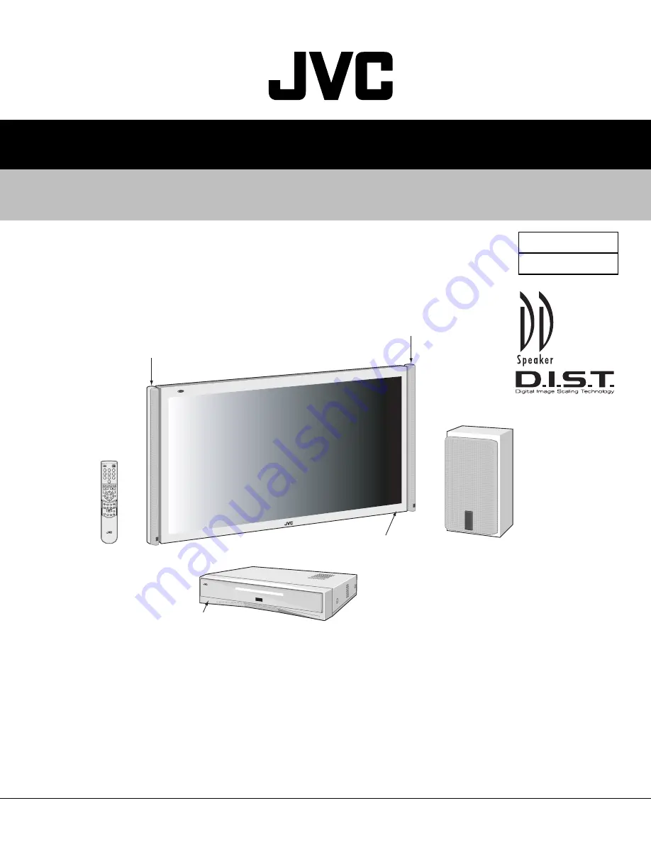
TS-42DX

[FRONT SPEAKER (R)]

TS-42DX

[FRONT SPEAKER (L)]

 TS-42DX

[SUB WOOFER]

[RM-C63]

VM-42DX

[PLASMA DISPLAY UNIT]

TU-42DX

[RECEIVER UNIT]

FREEZE

SUB-P

BASIC CHASSIS

MK

Summary of Contents for PD-42DX

Page 1: ...EVISION 52088 2003 02 PD 42DX TABLE OF CONTENTS 1 PRECAUTIONS 1 3 2 SPECIFIC SERVICE INSTRUCTIONS 1 6 3 ADJUSTMENTS 1 19 4 TROUBLE SHOOTING 1 46 TS 42DX FRONT SPEAKER R TS 42DX FRONT SPEAKER L TS 42DX SUB WOOFER RM C63 VM 42DX PLASMA DISPLAY UNIT TU 42DX RECEIVER UNIT FREEZE SUB P BASIC CHASSIS MK ...

Page 2: ... AC240V 50Hz 60Hz Power Consumption Plasma display unit Operate 338W Stand by 0 5W Receiver unit Operate 35W Stand by 2 4W Plasma Display Panel PDP QLE0020 001 42 inch wide aspect 16 9 Screen Size Viewable area 105 7cm measured diagonally W 92 1cm x H 51 8cm Display Pixels Horizontal 1024 dots x Vertical 768 dots XGA Audio Output Front 10W 10W Sub woofer 15W Speaker Front speaker Direct Drive syst...

Page 3: ...placements or alternatives approved by the manufacturer of the complete product 7 Do not check high voltage by drawing an arc Use a high voltage meter or a high voltage probe with a VTVM Discharge the picture tube before attempting meter connection by connecting a clip lead to the ground frame and connecting the other end of the lead through a 10k 2W resistor to the anode button 8 When service is ...

Page 4: ...as the floor etc Install the unit on stable flooring or stands Take precautionary measures to prevent the unit from tipping in order to protect against accidents and earthquakes 1 2 3 FALL TIP PREVENTION MEASURES Take precautionary measures to prevent the unit from falling or tipping to protect against emergencies such as earthquakes as well as accidents Fasten the supplied hook for tip fall preve...

Page 5: ...does not occur in the case of animated images When switching to another image after continuous display of the previous image residual images may become prominent as lu minance in a part of the display is higher than the other parts This is not a defect but is because due to the discharge surface of the lighted portion has becomebeing relatively activated and its luminance higher than the unlighted...

Page 6: ...t consist of DigiPure and picture motion compensation function PULL DOWN This function displays a cinema film picture more smoothly and naturally on the screen COLOUR MANAGEMENT This function ensures dull colours are compensated to produce natural hues Sleep Timer Setting for situations such as falling asleep while watching TV and for prevention against forgetting to turn off the TV The power supp...

Page 7: ...ases there may be defective pixels that do not light at all or the ones that always light on There are 2 types of Pixel defects Bright Dot Defects and Dark Dot Defects as defined respectively in the following 1 Bright Dot Defects Bright dot defect is a pixel cell that lights or blinks though it should not light The presence of bright dot defects can be confirmed by inputting a full black signal pa...

Page 8: ...DD33 I 3 3V 62 D13 D13 I O 63 D9 D9 I O 64 D5 D5 I O 65 D2 D2 I O 66 D12 D12 I O 67 D10 D10 I O 68 VSS33 VSS33 I GND 69 VDD33 VDD33 I 3 3V 70 D4 D4 I O 71 D3 D3 I O 72 D11 D11 I O 73 RESET IN RSTIN I 74 SCL0 P3 0 I O 75 SDA0 P3 1 I O 76 P3 2 I O 77 PIX_CLK P3 3 I O 78 AMP_MUTE P3 4 I O 79 AUDIO_MUTE P3 5 I O 80 READY P3 6 I O 81 STATUS P3 7 I O 82 DATA P3 8 I O 83 CLK P3 9 I O 84 VSS33 VSS33 I GND...

Page 9: ... 1 Remove the 4 screws F and remove the AUDIO PWB NOTE Disconnect the connectors CN60SP CN600K CN60CA CN60CE CN60CF from the AUDIO PWB It is advisable to take note of the connecting location connector number of the removed connectors 2 4 5 REMOVING THE SYSTEM POWER PWB Fig 3 Remove the REAR COVER Remove the TERMINAL COVER 1 Remove the 4 screws G and remove the SYSTEM POWER PWB NOTE Disconnect the ...

Page 10: ... Disconnect the connector CN0AH and earth wire from the DISPLAY INTERFACE PWB It is advisable to take note of the connecting location connector number of the removed connectors 3 Remove the 4 screws N and 5 screws O and remove the 2 pieces of SUPPORT BRACKET BOTTOM 4 Remove the 4 screws P and remove the 2 pieces of BACK FRAME BOTTOM 5 Remove the 4 screws Q and 1 screw R and remove the SUPPORT BRAC...

Page 11: ...O x2 P x2 S T x2 Q x2 Q R x4 U x2 N x2 O x2 P SUPPORT BRACKET BOTTOM TERMINAL BRACKET SUPPORT BRACKET BOTTOM BACK FRAME BOTTOM PANEL SHIELD BACK FRAME BOTTOM SUPPORT BRACKET TOP PDP UNIT FRONT PANEL INNER CASE FRONT FILTER TOP GAS insertion hole ...

Page 12: ...mpose shock to it 2 4 11 REMOVING THE DISPLAY SW PWB Fig 6 Remove the INNER CASE 1 Remove the 2 screws X and remove the DISPLAY LED PWB 2 4 12 REMOVING THE PANEL SW PWB Fig 6 Remove the INNER CASE 1 Remove the 2 screws Y and remove the CONTROL BASE 2 Remove the 3 screws Z and remove the DISPLAY SWITCH PWB 2 4 13 REMOVING THE FRONT FILTER Fig 6 Remove the INNER CASE 1 Remove the 10 screws a and rem...

Page 13: ...ction 2 5 6 REMOVING THE DIST PWB DIST RELAY PWB MI COM PWB MI COM INTERFACE PWB AV JACK PWB AV SW PWB and SUB TUNER PWB Remove the TOP COVER Remove the REAR COVER 1 Remove the 1 screw O and remove the PB HOLDER 2 Remove the 2 screws P and 2 screws Q Then lift up wards and withdraw the SUPPORT BRACKET the DIST PWB and the DIST RELAY PWB 3 Remove the 5 screws R and 1 screw S and remove the SUPPORT ...

Page 14: ...SIDE G DAMPER P D P Q Q R S W E E M N M L I J K O H T T x4 x4 U U V V V MAIN PWB AC INLET BACK COVER BOTTOM CASE FRONT CONTROL PWB RECEIVER POWER PWB AV SW PWB AV JACK PWB SUB TUNER PWB MI COM HOLDER MI COM PWB PB HOLDER MI COM INTERFACE PWB SUPPORT BRACKET DIST PWB DIST RELAY PWB x2 x2 x2 x14 x5 x2 INSULATOR C x1 ...

Page 15: ...y and MUTING key simultaneously Then the SYSTEM CONSTANT SET screen will be displayed See FIg 2 c Check whether the setting value of the SYSTEM CONSTANT SET is the same as these indicated in Table 1 d Press the INFORMATION key twice to return to the normal screen 5 Receive channel setting Refer to the OPERATING INSTRUCTIONS and set the re ceive channels 6 User setting Memories the user setting ite...

Page 16: ...UME 10 BALANCE Center PICTURE SETTING SPEAKER ON PICTURE MODE BRIGHT BBE OFF CONTRAST Center CINEMA SURROUND OFF BRIGHT Center SUBWOOFER LOW SHARP Center HEADPHONE COLOUR Center VOLUME 20 TINT Center TV SPEAKER OFF WHITE BALANCE MID OUTPUT MAIN PICTURE FEATURES VIDEO SETTING DIGITAL VNR AUTO ID LIST Super DigiPure AUTO FEATURES COLOUR SYSTEM TV Depend on PR CH EXT AUTO SLEEP TIMER OFF BLUE BACK ON...

Page 17: ... 7 TWIN HI R 19 B OF MB 6 YEGL 15 YCTL 8 TWIN HI B 20 B OF SR 7 YLTL 16 YNCL 9 BRIGHT 21 B OF SB 8 MCLV 17 YNCON 10 CONT S01 S97 9 MCGA 11 TWN BRG A01 A17 12 TWN CNT PDA01 PDA12 3 AUDIO Do not adjust 1 ERROR LIMIT 8 IP Do not adjust PPA001 PPA008 2 A2 ID THR PPB001 PPB036 3 Q PEAK PPC001 PPC007 4 SOUND LEVEL PPD001 PPD016 ADS001 ADS034 4 DD CM DDT01 DDT34 IPA001 IPA120 CMT01 CMT57 IPB001 IPB079 DD...

Page 18: ...th the tweezers and remove the chip part Transistors diodes variable resistors etc 1 Apply extra solder to each lead 2 As shown in the figure push the part with tweezers and alternately melt the solder at each lead Shift and remove the chip part Note After removing the part remove remaining solder from the pattern 2 How to install Chip parts Resistors capacitors etc 1 Apply solder to the pattern a...

Page 19: ...reen that are not stated in this manual 6 Unless otherwise stated in the ADJUSTMENT PROCEDURE section follow the settings for the features stated below using the remote control 3 2 MEASURING INSTRUMENT AND FIXTURES DC voltmeter or Digital voltmeter Oscilloscope Signal generator Pattern generator Remote control unit 3 3 MAIN PARTS LOCATIONS RECEIVER UNIT Fig 1 Setting item Settings PICTURE MODE STA...

Page 20: ...F901 LINE FILTER PWB AH SP CB CD CC CE CE SP CF CA K CB J P AT AV AU AV C2 C1 NC CF NC DISPALY SWITCH PWB AUDIO PWB SYSTEM POWER PWB PDP POWER PWB DISPLAY INTERFACE PWB SPEAKER TERMINAL PWB CN301 PDP UNIT CN302 PDP UNIT C4 POWER CONNECTOR THE CONNECTOR FOR ADJUSTMENT CN0 C4 DISPLAY LED PWB TOP CN104 PDP UNIT ...

Page 21: ... TINT WDR R WDR G WDR B Do not adjust Do not adjust OK 6 STATUS 1 SOFT 2 TELE TEXT 3 ASPECT 4 IC 5 DEBUG 6 PANEL 7 VNR 1 MYLV 2 ONMVF 3 MYCOR 4 MYGA 5 YEGON 6 YEGL 7 YLTL 8 MCLV 9 MCGA 10 MCCOR 11 CLTL 12 YNGA 13 COROF 14 LPF_OF 15 YCTL 16 TNCL 17 YNCON IP FULL PAL 8 IP STORE i EXIT PPA001 PPA008 PPB001 PPB036 PPC001 PPC007 PPD001 PPD016 ADS001 ADS034 IPA001 IPA120 IPB001 IPB088 IPC001 IPC044 IPD0...

Page 22: ...DURE Sets output data to the video circuit Function up down key For scrolling up down the item codes Function key For scrolling up down the data values 3 6 4 3 3 AUDIO SOUND setting Do not adjust 3 6 4 4 4 DD CM Panel picture processing setting Do not change settings of items that are not included in the ADJUSTMENT PROCEDURE Sets output data to the deflection circuit Function up down key For scrol...

Page 23: ...00 0000 0000 0000 11 TWN BRG 0000 0127 0081 0081 0081 0081 0081 0000 0000 0000 0000 12 TWN CNT 0000 0015 0007 0007 0007 0007 0007 0000 0000 0000 0000 13 COLOUR 0000 0015 0006 0006 0000 0000 0007 0000 0000 0000 0000 14 HUE 0000 0063 0007 0007 0000 0000 0034 0000 0000 0000 0063 15 BY GAIN 0000 0063 0032 0032 0000 0000 0043 0000 0000 0000 0043 16 TWN COL 0000 0015 0010 0010 0002 0002 0002 0002 0002 0...

Page 24: ...0 S40 NO DISPLAY 0000 0001 0001 0001 0001 S41 NO DISPLAY 0000 0001 0000 0000 0000 S42 NO DISPLAY 0000 0003 0001 0001 0001 S43 NO DISPLAY 0000 0031 0011 0011 0011 S44 NO DISPLAY 0000 0003 0001 0001 0001 S45 NO DISPLAY 0000 0003 0001 0001 0001 S46 NO DISPLAY 0000 0015 0015 0015 0015 S47 NO DISPLAY 0000 0015 0015 0015 0015 S48 NO DISPLAY 0000 0015 0015 0015 0015 S49 NO DISPLAY 0000 0001 0000 0000 000...

Page 25: ...0130 S87 NO DISPLAY 0000 0003 0001 0001 0001 S88 NO DISPLAY 0000 0007 0007 0007 0007 S89 NO DISPLAY 0000 0255 0030 0030 0030 S90 NO DISPLAY 0000 0127 0000 0000 0000 S91 NO DISPLAY 0000 0007 0007 0007 0007 S92 NO DISPLAY 0000 0031 0031 0031 0031 S93 NO DISPLAY 0000 0007 0007 0007 0007 S94 NO DISPLAY 0000 0031 0031 0031 0031 S95 NO DISPLAY 0000 0255 0060 0060 0060 S96 NO DISPLAY 0000 0015 0006 0006 ...

Page 26: ...0001 0000 0000 0000 PDA07 NO DISPLAY 0000 0255 0150 0150 0150 PDA08 NO DISPLAY 0000 0255 0150 0150 0150 PDA09 NO DISPLAY 0000 0255 0002 0002 0002 PDA10 NO DISPLAY 0000 0255 0060 0060 0060 PDA11 NO DISPLAY 0000 0255 0000 0000 0000 PDA12 NO DISPLAY 0000 0127 0000 0000 0000 Item No Item Variable range Setting value PAL SECAM 1 ERROR LIMIT 0000 0FF0 0100 0100 2 A2 ID THR 0000 00FF 0019 0019 3 Q PEAK 4...

Page 27: ...DT34 NO DISPLAY 0000 0255 0032 0032 0042 Item No Item Variable range Setting value PAL SECAM NTSC Item No Item Variable range Setting value PAL SECAM NTSC CMT01 NO DISPLAY 0000 0003 0000 0000 0000 CMT02 NO DISPLAY 0000 0255 0104 0104 0093 CMT03 NO DISPLAY 0000 0255 0020 0020 0010 CMT04 NO DISPLAY 0000 0255 0020 0020 0020 CMT05 NO DISPLAY 0000 0063 0062 0062 004 CMT06 NO DISPLAY 128 0127 0005 0005 ...

Page 28: ...AY 0000 0255 0080 0080 0000 CMT46 NO DISPLAY 0000 0001 0000 0000 0000 CMT47 NO DISPLAY 0000 0255 0070 0070 0128 CMT48 NO DISPLAY 0000 0001 0000 0000 0000 CMT49 NO DISPLAY 0000 0001 0001 0001 0001 CMT50 NO DISPLAY 0000 0031 0021 0021 0000 CMT51 NO DISPLAY 0000 0031 0021 0021 0000 CMT52 NO DISPLAY 0000 0001 0000 0000 0000 CMT53 NO DISPLAY 0000 0001 0000 0000 0000 CMT54 NO DISPLAY 0000 0003 0000 0000...

Page 29: ...Y 0000 0015 0010 0010 0010 DDP28 NO DISPLAY 0000 0015 0006 0006 0006 DDP29 NO DISPLAY 0000 0015 0010 0010 0010 DDP30 NO DISPLAY 0000 0015 0010 0010 0010 DDP31 NO DISPLAY 0000 0015 0006 0006 0006 DDP32 NO DISPLAY 0000 0255 0013 0013 0013 DDP33 NO DISPLAY 0000 0255 0133 0133 0133 DDP34 NO DISPLAY 0000 0255 0102 0102 0102 DDP35 NO DISPLAY 0000 0255 0144 0144 0144 DDP36 NO DISPLAY 0000 0255 0013 0013 ...

Page 30: ...F 000E 000E 000E 9 MCGA 0000 0003 0002 0002 0002 10 MCCOR 0000 001F 0003 0003 0003 11 CLTL 0000 007F 0009 0009 0009 12 YNGA 0000 0003 0003 0003 0003 13 COR_OF 0000 0001 0000 0000 0000 14 LPF_OF 0000 0001 0000 0000 0000 15 YCTL 0000 000F 0004 0004 0004 16 YNCL 0000 000F 000E 000E 000E 17 YNCON 0000 0001 0001 0001 0001 Item No Item Variable range Setting value PAL SECAM NTSC PPA001 NO DISPLAY 0000 0...

Page 31: ...Y 0000 001F 0000 0000 0000 PPB026 NO DISPLAY 0000 00FF 0000 0000 0000 PPB027 NO DISPLAY 0000 00FF 0000 0000 0000 PPB028 NO DISPLAY 0000 001F 0000 0000 0000 PPB029 NO DISPLAY 0000 00FF 0000 0000 0000 PPB030 NO DISPLAY 0000 00FF 0000 0000 0000 PPB031 NO DISPLAY 0000 001F 0000 0000 0000 PPB032 NO DISPLAY 0000 00FF 0000 0000 0000 PPB033 NO DISPLAY 0000 00FF 0000 0000 0000 PPB034 NO DISPLAY 0000 001F 0...

Page 32: ... 0028 0028 0028 ADS007 NO DISPLAY 0000 00FF 0096 0096 0096 ADS008 NO DISPLAY 0000 00FF 0020 0020 0020 ADS009 NO DISPLAY 0000 00FF 000FF 000FF 000FF ADS010 NO DISPLAY 0000 00FF 000FF 000FF 000FF ADS011 NO DISPLAY 0000 00FF 000FF 000FF 000FF ADS012 NO DISPLAY 0000 007F 004A 004A 004A ADS013 NO DISPLAY 0000 007F 0051 0051 0051 ADS014 NO DISPLAY 0000 007F 0042 0042 0042 ADS015 NO DISPLAY 0000 0001 000...

Page 33: ...001 0001 0001 0001 IPA018 NO DISPLAY 0000 003F 000B 000B 000B IPA019 NO DISPLAY 0000 0001 0001 0001 0001 IPA020 NO DISPLAY 0000 0001 0001 0001 0001 IPA021 NO DISPLAY 0000 003F 0030 0030 0030 IPA022 NO DISPLAY 0000 0003 0001 0001 0001 IPA023 NO DISPLAY 0000 003F 000A 000A 000A IPA024 NO DISPLAY 0000 0001 0001 0001 0001 IPA025 NO DISPLAY 0000 0001 0001 0001 0001 IPA026 NO DISPLAY 0000 003F 0030 0030...

Page 34: ...A066 NO DISPLAY 0000 003F 0008 0008 0008 IPA067 NO DISPLAY 0000 0001 0001 0001 0001 IPA068 NO DISPLAY 0000 003F 0007 0007 0007 IPA069 NO DISPLAY 0000 0003 0000 0000 0000 IPA070 NO DISPLAY 0000 00FF 0000 0000 0000 IPA071 NO DISPLAY 0000 000F 0005 0005 0005 IPA072 NO DISPLAY 0000 00FF 00DB 00DB 00DB IPA073 NO DISPLAY 0000 0001 0000 0000 0000 IPA074 NO DISPLAY 0000 0001 0000 0000 0000 IPA075 NO DISPL...

Page 35: ... DISPLAY 0000 000F 0000 0000 0000 IPA114 NO DISPLAY 0000 00FF 0000 0000 0000 IPA115 NO DISPLAY 0000 000F 0002 0002 0002 IPA116 NO DISPLAY 0000 00FF 00EF 00EF 00EF IPA117 NO DISPLAY 0000 0001 0000 0000 0000 IPA118 NO DISPLAY 0000 0001 0000 0000 0000 IPA119 NO DISPLAY 0000 0001 0000 0000 0000 IPA120 NO DISPLAY 0000 0001 0000 0000 0000 Item No Item Variable range Setting value PAL SECAM NTSC Item No ...

Page 36: ...B039 NO DISPLAY 0000 000F 0000 0000 0000 IPB040 NO DISPLAY 0000 000F 0000 0000 0000 IPB041 NO DISPLAY 0000 000F 0000 0000 0000 IPB042 NO DISPLAY 0000 00FF 0000 0000 0000 IPB043 NO DISPLAY 0000 000F 0000 0000 0000 IPB044 NO DISPLAY 0000 00FF 0000 0000 0000 IPB045 NO DISPLAY 0000 000F 0001 0001 0001 IPB046 NO DISPLAY 0000 00FF 008B 008B 008B IPB047 NO DISPLAY 0000 000F 0000 0000 0000 IPB048 NO DISPL...

Page 37: ...001 0000 0000 0000 IPC005 NO DISPLAY 0000 000F 0000 0000 0000 IPC006 NO DISPLAY 0000 00FF 0000 0000 0000 IPC007 NO DISPLAY 0000 000F 0005 0005 0005 IPC008 NO DISPLAY 0000 00FF 00DB 00DB 00DB IPC009 NO DISPLAY 0000 000F 0007 0007 0007 IPC010 NO DISPLAY 0000 00FF 00B9 00B9 00B9 IPC011 NO DISPLAY 0000 000F 0000 0000 0000 IPC012 NO DISPLAY 0000 00FF 0000 0000 0000 IPC013 NO DISPLAY 0000 0003 0000 0000...

Page 38: ...006 NO DISPLAY 0000 0007 0006 0006 0006 IPD007 NO DISPLAY 0000 00FF 0018 0018 0018 IPD008 NO DISPLAY 0000 0001 0000 0000 0000 IPD009 NO DISPLAY 0000 000F 0001 0001 0001 IPD010 NO DISPLAY 0000 00FF 0062 0062 0062 IPD011 NO DISPLAY 0000 000F 0005 0005 0005 IPD012 NO DISPLAY 0000 00FF 002B 002B 002B IPD013 NO DISPLAY 0000 0007 0000 0000 0000 IPD014 NO DISPLAY 0000 0007 0000 0000 0000 IPD015 NO DISPLA...

Page 39: ...D044 NO DISPLAY 0000 0001 0000 0000 0000 IPD045 NO DISPLAY 0000 0001 0000 0000 0000 IPD046 NO DISPLAY 0000 0001 0000 0000 0000 IPD047 NO DISPLAY 0000 00FF 0000 0000 0000 IPD048 NO DISPLAY 0000 00FF 0000 0000 0000 IPD049 NO DISPLAY 0000 00FF 0090 0090 0090 IPD050 NO DISPLAY 0000 0007 0000 0000 0000 IPD051 NO DISPLAY 0000 00FF 001D 001D 001D IPD052 NO DISPLAY 0000 0007 0002 0002 0002 IPD053 NO DISPL...

Page 40: ... voltage between pins 5 and 6 of CN0C4 5V coincides with the values in the table 5 Turn off the power and connect the CN0AT and CN0AU connectors and turn on the power again 6 Input a PAL 625i all black signal and check that it coincides with the values in the table 7 If the adjusted value is different from those in the table fine tune without unplugging the connectors CAUTION Designated power supp...

Page 41: ...unit Signal generator 2 V C 9 BRIGHT Bright 1 Receive a PAL black and white pattern signal including 0 black signal 2 Select 2 V C from the SERVICE MENU 3 Adjust 9 BRIGHT Bright to set the 0 black part to be the brightest 4 Press the OK key to save the value SUB CONTRAST Remote control unit Signal generator 2 V C 10 CONT Contrast 1 Receive a PAL black and white pattern signal colour off 2 Select 2...

Page 42: ...al screen SECAM COLOUR 6 Receive a SECAM colour bar signal half colour bar 7 Select 2 V C from the SERVICE MENU 8 Make similar adjustment of SECAM COLOUR in the same way as for PAL COLOUR See Fig 5 NTSC COLOUR 9 Input a NTSC 3 58 colour bar signal full field colour bar 75 white 10 Select 2 V C from the SERVICE MENU 11 Make similar adjustment of NTSC COLOUR in the same way as for PAL COLOUR See Fig...

Page 43: ...in the upper half of the sub right screen See Fig 6 NOTE If you select an adjustment item 7 TWN HI R then the screen automatically turns to twin pic tures mode 4 Press the OK key to save the value 5 Adjust 8 TWN HI B Sub screen high light blue to minimize the blue noise in the upper half of the sub right screen See Fig 6 6 Press the OK key to save the value Fig 6 SUB SCREEN CONTRAST Remote control...

Page 44: ...B SCREEN SECAM COLOUR 6 Receive a SECAM colour bar signal half colour bar 7 Select 2 V C from the SERVICE MENU 8 Make similar adjustment of SECAM COLOUR in the same way as for SUB SCREEN PAL COLOUR See Fig 8 SUB SCREEN NTSC COLOUR 9 Input a NTSC 3 58 composite colour bar signal full field colour bar 75 white 10 Select 2 V C from the SERVICE MENU 11 Make similar adjustment of NTSC COLOUR in the sam...

Page 45: ...ffset 1 Input a picture whose signal synchronization state is stable 2 Select 4 DD CM from the SERVICE MENU 3 Select OSD G OSD green offset If you select OSD G then the screen turns to OSD adjustment mode See Fig 9 4 Adjust OSD G OSD green offset OSD B OSD blue offset and OSD R OSD red offset so that OSD background is in the same colour as its surroundings When the background is in green fix OSD G...

Page 46: ...r is turned off and turns to stand by state Receiver Abnormal rise of temperature in audio part of Display unit TH6671 AUDIO PWB RED Flash every 1 0 second RED Flash0 1second Out0 1second Detection is performed every 1 second The power is turned off if the temperature sensor operates for 10 seconds or longer Display Abnormal power supply in PDP PANEL short circuit etc PDP RED Flash every 1 0 secon...

Page 47: ...PD 42DX No 52088 1 47 ...

Page 48: ... No 52088 AV MULTIMEDIA COMPANY DISPLAY CATEGORY 12 3 chome Moriya cho kanagawa ku Yokohama kanagawa prefecture 221 8528 Japan VICTOR COMPANY OF JAPAN LIMITED 200302WPC Printed in Japan PD 42DX ...

Reviews: