Jäger ADwin-Gold, Hardware Manual
The User's Reference Manual for the FTA ADwin-Gold is a comprehensive guide designed to help users maximize the potential of this powerful product. Available for free download from our website, this manual provides detailed instructions and information to enhance your experience with the FTA ADwin-Gold.
Share
Download


Reviews:
No comments
Related manuals for ADwin-Gold

DRC1
Brand: Dantherm Pages: 96

SMV
Brand: Aalborg Pages: 15

DFC
Brand: Aalborg Pages: 48

S9500E Series
Brand: H3C Pages: 5

WX3500H series
Brand: H3C Pages: 4

TLS
Brand: Veeder-Root Pages: 27

1078
Brand: Valve Concepts Pages: 18
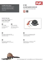
M1500
Brand: K&K Pages: 6

1E0671-1 MCR2.9
Brand: Haberl Electronic Pages: 9

J4C Series
Brand: J+J Pages: 2

Sentinel S4
Brand: Apricus Pages: 32

WBR3L
Brand: TUYA Pages: 28

MultiLoad II EXL
Brand: Toptech Pages: 83

R8-YS2
Brand: M-system Pages: 4

AT91 ARM Thumb
Brand: Atmel Pages: 12

MK5 NX w/ACC
Brand: Invacare Pages: 44

Tacosol Load EXA L
Brand: Taconova Pages: 40

Veritas R8 Plus
Brand: Texecom Pages: 8


