background image

*

Other brands and names are the property of their respective owners.

Information in this document is provided in connection with Intel products. Intel assumes no liability whatsoever, including infringement of any patent or
copyright, for sale and use of Intel products except as provided in Intel’s Terms and Conditions of Sale for such products. Intel retains the right to make
changes to these specifications at any time, without notice. Microcomputer Products may have minor variations to this specification known as errata.

October 1995

COPYRIGHT

©

INTEL CORPORATION, 1995

Order Number: 272433-004

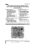
80C186EB/80C188EB AND 80L186EB/80L188EB

16-BIT HIGH-INTEGRATION EMBEDDED PROCESSORS

X

Full Static Operation

X

True CMOS Inputs and Outputs

Y

Integrated Feature Set
РLow-Power Static CPU Core
РTwo Independent UARTs each with

an Integral Baud Rate Generator

РTwo 8-Bit Multiplexed I/O Ports
РProgrammable Interrupt Controller
РThree Programmable 16-Bit

Timer/Counters

РClock Generator
РTen Programmable Chip Selects with

Integral Wait-State Generator

РMemory Refresh Control Unit
РSystem Level Testing Support (ONCE

Mode)

Y

Direct Addressing Capability to 1 Mbyte
Memory and 64 Kbyte I/O

Y

Speed Versions Available (5V):
Р25 MHz (80C186EB25/80C188EB25)
Р20 MHz (80C186EB20/80C188EB20)
Р13 MHz (80C186EB13/80C188EB13)

Y

Available in Extended Temperature
Range (

b

40

§

C to

a

85

§

C)

Y

Speed Versions Available (3V):
Р16 MHz (80L186EB16/80L188EB16)
Р13 MHz (80L186EB13/80L188EB13)
Р8 MHz (80L186EB8/80L188EB8)

Y

Low-Power Operating Modes:
РIdle Mode Freezes CPU Clocks but

keeps Peripherals Active

РPowerdown Mode Freezes All

Internal Clocks

Y

Supports 80C187 Numeric Coprocessor
Interface (80C186EB PLCC Only)

Y

Available In:
Р80-Pin Quad Flat Pack (QFP)
Р84-Pin Plastic Leaded Chip Carrier

(PLCC)

Р80-Pin Shrink Quad Flat Pack (SQFP)

The 80C186EB is a second generation CHMOS High-Integration microprocessor. It has features that are new
to the 80C186 family and include a STATIC CPU core, an enhanced Chip Select decode unit, two independent
Serial Channels, I/O ports, and the capability of Idle or Powerdown low power modes.

272433 – 1

Summary of Contents for 80C186EB

Page 1: ...6 Bit Timer Counters Clock Generator Ten Programmable Chip Selects with Integral Wait State Generator Memory Refresh Control Unit System Level Testing Support ONCE Mode Y Direct Addressing Capability...

Page 2: ...8 Prefix Identification 8 Pin Descriptions 8 80C186EB PINOUT 14 PACKAGE THERMAL SPECIFICATIONS 22 ELECTRICAL SPECIFICATIONS 23 Absolute Maximum Ratings 23 CONTENTS PAGE Recommended Connections 23 DC...

Page 3: ...80C186EB 80C188EB 80L186EB 80L188EB 272433 2 NOTE Pin names in parentheses apply to the 80C188EB 80L188EB Figure 1 80C186EB 80C188EB Block Diagram 3...

Page 4: ...d up effective address calculations enhance execution speed for multiple bit shift and rotate in structions and for multiply and divide instructions string move instructions that operate at full bus b...

Page 5: ...ary Figure 3 provides a list of the registers associated with the PCB The Register Bit Summary at the end of this specification individually lists all of the regis ters and identifies each of their pr...

Page 6: ...Serial0 RBUF 6AH Serial0 TBUF 6CH Reserved 6EH Reserved 70H Serial1 Baud 72H Serial1 Count 74H Serial1 Control 76H Serial1 Status 78H Serial1 RBUF 7AH Serial1 TBUF 7CH Reserved 7EH Reserved PCB Functi...

Page 7: ...ontrol Unit The Refresh Control Unit RCU automatically gen erates a periodic memory read bus cycle to keep dynamic or pseudo static memory refreshed A 9 bit counter controls the number of clocks betwe...

Page 8: ...utput only O or input output I O Some pins have multiplexed functions for example A19 S6 Additional symbols indicate additional characteristics for each pin Table 2 lists all the possible symbols for...

Page 9: ...ent State during Bus Hold R WH Output Weakly Held at VCC during Reset R 1 Output Driven to VCC during Reset R 0 Output Driven to VSS during Reset R Z Output Floats during Reset R Q Output Remains Acti...

Page 10: ...and assume an initialized state All pins will be driven to a known state and RESOUT will also be driven active The rising edge low to high transition synchronizes CLKOUT with CLKIN before the processo...

Page 11: ...atch Enable output is used to strobe address information into a transparent type latch during the address phase R 0 of the bus cycle P 0 BHE O H Z Byte High Enable output to indicate that the bus cycl...

Page 12: ...cates the last numerics coprocessor operation resulted in an exception condition An interrupt N C TYPE 16 is generated if ERROR is sampled active at the beginning of a numerics operation ERROR is not...

Page 13: ...s P2 6 R Z P X CTSO I A L Clear To Send input is used to prevent the transmission of serial data on their respective TXD P2 4 CTS1 signal pin CTS1 is multiplexed with an input only port function TXD0...

Page 14: ...e contacts facing down Table 4 PLCC Pin Names with Package Location Address Data Bus Name Location AD0 61 AD1 66 AD2 68 AD3 70 AD4 72 AD5 74 AD6 76 AD7 78 AD8 A8 62 AD9 A9 67 AD10 A10 69 AD11 A11 71 A...

Page 15: ...T1 33 INT2 INTA0 34 INT3 INTA1 35 INT4 36 PDTMR 37 RESIN 38 RESOUT 39 PEREQ N C 40 OSCOUT 41 CLKIN 42 VCC Location Name 43 VSS 44 CLKOUT 45 T0OUT 46 T0IN 47 T1OUT 48 T1IN 49 P2 7 50 P2 6 51 CTS0 52 TX...

Page 16: ...80C188EB 80L186EB 80L188EB 272433 5 NOTE This is the FPO number location indicated by X s Pin names in parentheses apply to the 80C188EB 80L188EB Figure 4 84 Pin Plastic Leaded Chip Carrier Pinout Di...

Page 17: ...OCK 47 HOLD 45 HLDA 44 Power Name Location VSS 12 14 33 35 53 73 VCC 13 34 54 72 Processor Control Name Location RESIN 68 RESOUT 69 CLKIN 71 OSCOUT 70 CLKOUT 74 TEST 46 PDTMR 67 NMI 48 INT0 62 INT1 63...

Page 18: ...AD15 A15 29 A16 30 A17 31 A18 32 A19 ONCE 33 VSS 34 VCC 35 VSS 36 RD 37 WR 38 ALE 39 BHE RFSH 40 S2 Location Name 41 S1 42 S0 43 DEN 44 HLDA 45 HOLD 46 TEST 47 LOCK 48 NMI 49 READY 50 P1 7 GCS7 51 P1...

Page 19: ...80C186EB 80C188EB 80L186EB 80L188EB 272433 6 NOTE This is the FPO number location indicated by X s Pin names in parentheses apply to the 80C188EB 80L188EB Figure 5 Quad Flat Pack Pinout Diagram 19...

Page 20: ...6 P2 3 SINT1 42 P2 4 CTS1 43 P2 5 BCLK0 41 P2 6 37 P2 7 36 CTS0 38 TXD0 39 RXD0 40 T0IN 33 T1IN 35 T0OUT 32 T1OUT 34 Table 9 SQFP Pin Locations with Pin Names 1 HLDA 2 HOLD 3 TEST 4 LOCK 5 NMI 6 READY...

Page 21: ...80C186EB 80C188EB 80L186EB 80L188EB 272433 7 NOTE XXXXXXXXC indicates Intel FPO number Pin names in parentheses apply to the 80C188EB 80L188EB Figure 6 SQFP Package 21...

Page 22: ...he top surface TA the ambient temperature can be calculated from iCA thermal resistance from the case to ambi ent with the following equation TA e TC b P iCA Typical values for iCA at various airflows...

Page 23: ...nnections must be made to multiple VCC and VSS pins Every 80C186EB based circuit board should include separate power VCC and ground VSS planes Every VCC pin must be connected to the power plane and ev...

Page 24: ...5 100 mA Notes 5 7 80C186EB20 100 mA Note 5 80C186EB13 100 mA Note 5 CIN Input Pin Capacitance 0 15 pF TF e 1 MHz COUT Output Pin Capacitance 0 15 pF TF e 1 MHz Note 6 NOTES 1 These pins have an inter...

Page 25: ...Input Pin Capacitance 0 15 pF TF e 1 MHz COUT Output Pin Capacitance 0 15 pF TF e 1 MHz Note 7 NOTES 1 IOL and IOH measured at VCC e 3 0V 2 These pins have an internal pull up device that is active wh...

Page 26: ...t Powerdown 5 5V 80L186EB13 100 mA Note 6 80L186EB8 100 mA Note 6 IPD3 Supply Current Powerdown 2 7V 80L186EB13 30 mA Note 6 80L186EB8 30 mA Note 6 CIN Input Pin Capacitance 0 15 pF TF e 1 MHz COUT Ou...

Page 27: ...ween the as sertion of NMI and the enabling of the internal clocks when exiting Powerdown A delay is required only when using the on chip oscillator to allow the crystal or resonator circuit time to s...

Page 28: ...0 16 ns 1 4 T CLKOUT Period 2 TC ns 1 TPH CLKOUT High Time T 2 b 5 T 2 a 5 ns 1 TPL CLKOUT Low Time T 2 b 5 T 2 a 5 ns 1 TPR CLKOUT Rise Time 1 6 ns 1 5 TPF CLKOUT Fall Time 1 6 ns 1 5 OUTPUT DELAYS T...

Page 29: ...OTES 1 See AC Timing Waveforms for waveforms and definition 2 Measure at VIH for high time VIL for low time 3 Only required to guarantee ICC Maximum limits are bounded by TC TCH and TCL 4 Specified fo...

Page 30: ...4 T CLKOUT Period 2 TC 2 TC ns 1 TPH CLKOUT High Time T 2 b 5 T 2 a 5 T 2 b 5 T 2 a 5 ns 1 TPL CLKOUT Low Time T 2 b 5 T 2 a 5 T 2 b 5 T 2 a 5 ns 1 TPR CLKOUT Rise Time 1 6 1 6 ns 1 5 TPF CLKOUT Fall...

Page 31: ...EQ ERROR 3 3 ns 1 9 NOTES 1 See AC Timing Waveforms for waveforms and definition 2 Measure at VIH for high time VIL for low time 3 Only required to guarantee ICC Maximum limits are bounded by TC TCH a...

Page 32: ...KOUT High Time T 2 b 5 T 2 a 5 ns 1 TPL CLKOUT Low Time T 2 b 5 T 2 a 5 ns 1 TPR CLKOUT Rise Time 1 9 ns 1 5 TPF CLKOUT Fall Time 1 9 ns 1 5 OUTPUT DELAYS TCHOV1 DT R LOCK A19 16 RFSH 3 22 ns 1 4 6 7...

Page 33: ...C Timing Waveforms for waveforms and definition 2 Measure at VIH for high time VIL for low time 3 Only required to guarantee ICC Maximum limits are bounded by TC TCH and TCL 4 Specified for a 50 pF lo...

Page 34: ...4 T CLKOUT Period 2 TC 2 TC ns 1 TPH CLKOUT High Time T 2 b 5 T 2 a5 T 2 b 5 T 2 a5 ns 1 TPL CLKOUT Low Time T 2 b 5 T 2 a 5 T 2 b 5 T 2 a 5 ns 1 TPR CLKOUT Rise Time 1 10 1 15 ns 1 5 TPF CLKOUT Fall...

Page 35: ...s 1 9 NOTES 1 See AC Timing Waveforms for waveforms and definition 2 Measured at VIH for high time VIL for low time 3 Only required to guarantee ICC Maximum limits are bounded by TC TCH and TCL 4 Spec...

Page 36: ...ing to RD Falling 2T b 15 ns 1 TWHLH WR Rising to ALE Rising 2T b 10 ns 1 TAFRL Address Float to RD Falling 0 ns TRLRH RD Falling to RD Rising 2 T b 5 ns 2 TWLWH WR Falling to WR Rising 2 T b 5 ns 2 T...

Page 37: ...ck High to Clock Low n e 1 T b 35 T a 35 ns 1 TQVXH RXD Output Data Setup to TXD Clock High n l 1 n b 1 T b 35 ns 1 2 TQVXH RXD Output Data Setup to TXD Clock High n e 1 T b 35 ns 1 TXHQX RXD Output D...

Page 38: ...ection to see how timings vary with load capacitance Specifications are measured at the VCC 2 crossing point unless otherwise specified See AC Timing Waveforms for AC specification definitions test pi...

Page 39: ...80C186EB 80C188EB 80L186EB 80L188EB 272433 10 NOTE 20 VCC k Float k 80 VCC Figure 9 Output Delay and Float Waveform 272433 11 Figure 10 Input Setup and Hold 39...

Page 40: ...80C186EB 80C188EB 80L186EB 80L188EB 272433 12 NOTE Pin names in parentheses apply to 80C188EB 80L188EB Figure 11 Relative Signal Waveform 272433 13 Figure 12 Serial Port Mode 0 Waveform 40...

Page 41: ...86EB 80C188EB 80L186EB 80L188EB DERATING CURVES TYPICAL OUTPUT DELAY VARIATIONS VERSUS LOAD CAPACITANCE 272433 14 Figure 13 TYPICAL RISE AND FALL VARIATIONS VERSUS LOAD CAPACITANCE 272433 15 Figure 14...

Page 42: ...ble the length of time is application specific and de pends on the startup characteristics of the crystal circuit The RESIN pin is designed to operate cor rectly using an RC reset circuit but the desi...

Page 43: ...nization occurs on the rising edge of RESIN If RESIN is sampled high while CLKOUT is high solid line then CLKOUT will remain low for two CLKIN periods If RESIN is sampled high while CLKOUT is low dash...

Page 44: ...nization occurs on the rising edge of RESIN If RESIN is sampled high while CLKOUT is high solid line then CLKOUT will remain low for two CLKIN periods If RESIN is sampled high while CLKOUT is low dash...

Page 45: ...own in the figure is the relationship of the various bus signals to CLKOUT These figures along with the information present in AC Specifications allow the user to determine all the critical timing ana...

Page 46: ...80C186EB 80C188EB 80L186EB 80L188EB 272433 19 NOTE Pin names in parentheses apply to 80C188EB 80L188EB Figure 18 Write Cycle Waveforms 46...

Page 47: ...f the next instruction prefetch Under a majority of instruction sequences the AD15 0 AD7 0 bus will float while the A19 16 A19 8 bus remains driven and all bus control signals are driven to their inac...

Page 48: ...80C186EB 80C188EB 80L186EB 80L188EB 272433 21 NOTE Pin names in parentheses apply to 80C188EB 80L188EB Figure 20 Interrupt Acknowledge Cycle Waveform 48...

Page 49: ...80C186EB 80C188EB 80L186EB 80L188EB 272433 22 NOTE Pin names in parentheses apply to 80C188EB 80L188EB Figure 21 HOLD HLDA Waveforms 49...

Page 50: ...433 23 NOTES 1 READY must be low by either edge to cause a wait state 2 Lighter lines indicate READ cycles darker lines indicate WRITE cycles Pin names in parentheses apply to 80C188EB 80L188EB Figure...

Page 51: ...88EB 272433 24 NOTES 1 READY must be low by either edge to cause a wait state 2 Lighter lines indicate READ cycles darker lines indicate WRITE cycles Pin names in parentheses apply to 80C188EB 80L188E...

Page 52: ...me required to fetch the opcode of the next instruction at the destination address All instructions which involve memory accesses can require one or two additional clocks above the mini mum timings sh...

Page 53: ...A e Push All 0 1 1 0 0 0 0 0 36 68 POP e Pop Memory 1 0 0 0 1 1 1 1 mod 0 0 0 r m 20 24 Register 0 1 0 1 1 reg 10 14 Segment register 0 0 0 reg 1 1 1 regi01 8 12 POPA e Pop All 0 1 1 0 0 0 0 1 51 83 X...

Page 54: ...ata if we1 3 4 3 4 8 16 bit SBB e Subtract with borrow Reg memory and register to either 0 0 0 1 1 0 d w mod reg r m 3 10 3 10 Immediate from register memory 1 0 0 0 0 0 s w mod 0 1 1 r m data data if...

Page 55: ...0 1 0 0 0 w mod TTT r m 2 15 2 15 Register Memory by CL 1 1 0 1 0 0 1 w mod TTT r m 5an 17an 5an 17an Register Memory by Count 1 1 0 0 0 0 0 w mod TTT r m count 5an 17an 5an 17an TTT Instruction 0 0...

Page 56: ...1 0 1 0 0 1 1 w 5a22n 5a22n SCAS e Scan string 1 1 1 1 0 0 1 z 1 0 1 0 1 1 1 w 5a15n 5a15n LODS e Load string 1 1 1 1 0 0 1 0 1 0 1 0 1 1 0 w 6a11n 6a11n STOS e Store string 1 1 1 1 0 0 1 0 1 0 1 0 1...

Page 57: ...NLE JG e Jump on not less or equal greater 0 1 1 1 1 1 1 1 disp 4 13 4 13 JNB JAE e Jump on not below above or equal 0 1 1 1 0 0 1 1 disp 4 13 4 13 JNBE JA e Jump on not below or equal above 0 1 1 1 0...

Page 58: ...n DISP e disp low sign ex tended to 16 bits disp high is absent if mod e 10 then DISP e disp high disp low if r m e 000 then EA e BX a SI a DISP if r m e 001 then EA e BX a DI a DISP if r m e 010 then...

Page 59: ...r than TCD 4 RESIN has a hysterisis of only 130 mV It is rec ommended that RESIN be driven by a Schmitt triggered device to avoid processor lockup during reset using an RC circuit 5 SINT1 will only go...

Reviews: