Iiyama Vision Master Pro 450, Service Manual
The Iiyama Vision Master Pro 450 is a high-quality monitor designed for professionals. To ensure that you get the most out of this product, we offer a comprehensive Service Manual for free download on our website. Simply visit manualshive.com to get this manual and maximize your user experience.
Share
Download


Reviews:
No comments
Related manuals for Vision Master Pro 450

TH-47LFT30W
Brand: Panasonic Pages: 3

TH-42PRT12U
Brand: Panasonic Pages: 36

TH-32EF2U
Brand: Panasonic Pages: 23

TH-42PH12L
Brand: Panasonic Pages: 26

PT51HX41E - 51" PROJECTION TV
Brand: Panasonic Pages: 61

TH-103VX200W
Brand: Panasonic Pages: 4

E110I
Brand: Panasonic Pages: 52

CYVM5800U - 5.8" CLR MONITOR/DVD
Brand: Panasonic Pages: 3

PLCD42HD
Brand: Panasonic Pages: 2

TH-37PW7BX
Brand: Panasonic Pages: 127

CFVDW07M - COMPUTER WIRELESS DISPLAY
Brand: Panasonic Pages: 30

CF-VDW07HM
Brand: Panasonic Pages: 4

TH-103PF10EK
Brand: Panasonic Pages: 56

GT series
Brand: Panasonic Pages: 136

BT-LH2550
Brand: Panasonic Pages: 12

CF-08TX1A1M
Brand: Panasonic Pages: 68

PL Series
Brand: Wacom Pages: 26
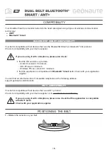
Dual Belt Bluetooth Smart / ANT+
Brand: GEONAUTE Pages: 5


