background image


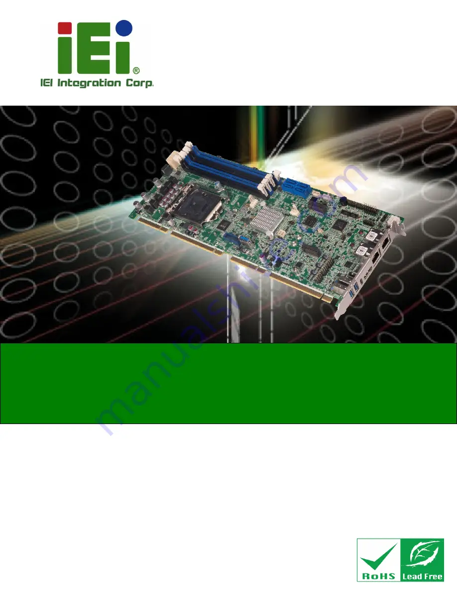
PCIE-Q470 Full-size PICMG 1.3 CPU Card 

Page  1 

User Manual 


Rev. 1.00 

 May 18, 2022 


Full-size PICMG 1.3 CPU Card supports LGA1200 10th/11th 

Generation Intel® Core™ i9/i7/i5/i3, Pentium®, Celeron® 

Processor with Intel® Q470/Q470E, DDR4, HDMI, Dual Intel® 

2.5GbE, USB 3.2, SATA6Gb/s, M.2, iAUDIO and RoHS


MODEL: 

PCIE-Q470 

Summary of Contents for PCIE-Q470

Page 1: ...er Manual Rev 1 00 May 18 2022 Full size PICMG 1 3 CPU Card supports LGA1200 10th 11th Generation Intel Core i9 i7 i5 i3 Pentium Celeron Processor with Intel Q470 Q470E DDR4 HDMI Dual Intel 2 5GbE USB 3 2 SATA6Gb s M 2 iAUDIO and RoHS MODEL PCIE Q470 ...

Page 2: ...PCIE Q470 Full size PICMG 1 3 CPU Card Page 2 Revision Date Version Changes May 18 2022 1 00 Initial release ...

Page 3: ...l damages arising out of the use or inability to use the product or documentation even if advised of the possibility of such damages This document contains proprietary information protected by copyright All rights are reserved No part of this manual may be reproduced by any mechanical electronic or other means in any form without prior written permission of the manufacturer TRADEMARKS All register...

Page 4: ...personal injury Warnings should be taken seriously CAUTION Cautionary messages should be heeded to help reduce the chance of losing data or damaging the product NOTE These messages inform the reader of essential but non critical information These messages should be read carefully as any directions or instructions contained therein can help avoid making mistakes ...

Page 5: ...NECTORS 25 3 1 PERIPHERAL INTERFACE CONNECTORS 26 3 1 1 PCIE Q470 Layout 26 3 1 2 Peripheral Interface Connectors 27 3 1 3 External Interface Panel Connectors 28 3 2 INTERNAL PERIPHERAL CONNECTORS 29 3 2 1 CPU 12V Power Connector 29 3 2 2 Battery Connector 30 3 2 3 Chassis Intrusion Connector 31 3 2 4 Digital Input Output Connector 32 3 2 5 EC Debug Connector 33 3 2 6 Fan Connectors CPU 34 3 2 7 F...

Page 6: ...nal USB 3 2 Gen 1 Connector 57 3 3 EXTERNAL PERIPHERAL INTERFACE CONNECTOR PANEL 58 3 3 1 External 2 5GbE RJ 45 connectors 59 3 3 2 External HDMI connector 60 3 3 3 External USB 3 2 Gen 1 Connectors Type A 61 3 3 4 External USB 3 2 Gen 2 Connector Type C 62 4 INSTALLATION 63 4 1 ANTI STATIC PRECAUTIONS 64 4 2 INSTALLATION CONSIDERATIONS 64 4 3 SOCKET LGA1200 CPU INSTALLATION 66 4 4 SOCKET LGA1200 ...

Page 7: ...FTWARE INSTALLATION 79 4 8 1 Driver Download 79 4 9 INTEL AMT SETUP PROCEDURE 81 A REGULATORY COMPLIANCE 82 B PRODUCT DISPOSAL 84 C ERROR BEEP CODE 86 C 1 PEI BEEP CODES 87 C 2 DXE BEEP CODES 87 D HAZARDOUS MATERIALS DISCLOSURE 88 D 1 ROHS II DIRECTIVE 2015 863 EU 89 D 2 CHINA ROHS 90 ...

Page 8: ...n 37 Figure 3 11 I2 C Connector Location 38 Figure 3 12 SMBus Connector Location 39 Figure 3 13 LAN LED Connector Locations 40 Figure 3 14 M 2 A key 2230 Slot Location 41 Figure 3 15 M 2 B key 3042 3052 2242 2280 Slot Location 43 Figure 3 16 M 2 M key 2242 2280 Slot Location 45 Figure 3 17 Power Button Location 47 Figure 3 18 DDR4 DIMM Socket Locations 48 Figure 3 19 SATA 6Gb s Connector Locations...

Page 9: ...ad Lever 66 Figure 4 2 Remove Protective Cover 67 Figure 4 3 Insert the Socket LGA1200 CPU 68 Figure 4 4 Close the Socket LGA1200 68 Figure 4 5 Cooling Kit Support Bracket 70 Figure 4 6 DIMM Installation 71 Figure 4 7 AT ATX Power Mode Switch Location 72 Figure 4 8 BIOS Switch Locations 73 Figure 4 9 Clear CMOS Button Location 74 Figure 4 10 Flash Descriptor Security Override Jumper Location 75 Fi...

Page 10: ...ble 3 11 I2 C Connector Pinouts 38 Table 3 12 SMBus Connector Pinouts 39 Table 3 13 LAN LED Connector Pinouts 40 Table 3 14 M 2 A key 2230 Slot Pinouts 42 Table 3 15 M 2 B key 3042 3052 2242 2280 Slot Pinouts 44 Table 3 16 M 2 M key 2242 2280 Slot Pinouts 46 Table 3 17 SATA 6Gb s Connector Pinouts 49 Table 3 18 RS 232 Serial Port Connector Pinouts 50 Table 3 19 RS 422 485 Serial Port Connectors Pi...

Page 11: ... A Pinouts 61 Table 3 31 USB 3 2 Gen 2 Type C Port Pinouts 62 Table 4 1 AT ATX Power Mode Switch Settings 72 Table 4 2 BIOS Switch Settings 73 Table 4 3 PCIe x16 Channel Mode Setup 74 Table 4 4 Flash Descriptor Security Override Jumper Settings 75 Table 4 5 BIOS Options and Configured USB Ports 76 Table 4 6 USB Power Source Setup 76 ...

Page 12: ...PCIE Q470 Full size PICMG 1 3 CPU Card Page 12 Chapter 1 1 Introduction ...

Page 13: ...s up to 128 GB The integrated Intel Q470 Q470E chipset supports four SATA 6Gb s drives with RAID 0 1 5 10 function The PCIE Q470 provides two 2 5GbE interfaces through the Intel I225V controllers Expansion and I O include three M 2 slots two USB 3 2 Gen 1 ports and one USB 3 2 Gen 2 by USB Type C port on the rear panel six USB 2 0 via internal pin headers two USB 3 2 Gen 1 via internal box headers...

Page 14: ...Express Generation 3 0 One M 2 2280 M key slot for storage Four SATA 6Gb s connectors support RAID 0 1 5 10 function Two USB 3 2 Gen 1 by USB Type A ports on the rear I O One USB 3 2 Gen 2 by USB Type C port on the rear I O Six USB 2 0 ports via internal pin headers Two USB 3 2 Gen1 ports via internal box headers One USB 3 2 Gen1 via internal Type A connector Two RS 232 serial ports via internal p...

Page 15: ...PCIE Q470 Full size PICMG 1 3 CPU Card Page 15 1 3 Connectors The connectors on the PCIE Q470 are shown in the figure below Figure 1 2 Connectors ...

Page 16: ...PCIE Q470 Full size PICMG 1 3 CPU Card Page 16 1 4 Dimensions The main dimensions of the PCIE Q470 are shown in the diagram below Figure 1 3 PCIE Q470 Dimensions mm ...

Page 17: ...IE Q470 Full size PICMG 1 3 CPU Card Page 17 1 5 Data Flow Figure 1 4 shows the data flow between the system chipset the CPU and other components installed on the motherboard Figure 1 4 Data Flow Diagram ...

Page 18: ...its supporting DX2015 OpenGL 5 X and OpenCL2 x ES 2 0 11th Generation RKL SXe 12th Generation Graphics Architecture Intel UHD Graphics 750 supports 12 bit end to end support AV1 VP9 HEVC 12b HDR10 FP16 Display Output 1 x HDMI 1 4 up to 4096 x 2160 30Hz Ethernet Controllers LAN1 Intel I225V 2 5GbE controller LAN2 Intel I225V 2 5GbE controller Audio 1 x iAUDIO support IEI AC KIT 888S Audio Module 2 ...

Page 19: ...D HDD LED power button reset button I2 C One 4 pin wafer connector Keyboard and Mouse One internal keyboard and mouse connector 6 pin wafer LAN LED Two 2 pin headers for LAN1 LED and LAN2 LED Serial ATA 4 x SATA 6Gb s connectors support RAID 0 1 5 10 Serial Ports 2 x RS 232 2x5 pin P 2 0 2 x RS 422 485 1x4 pin P 2 0 support AFC SMBus One 4 pin wafer connector TPM Intel PTT TPM 2 0 USB Ports 2 x US...

Page 20: ...on 3 3V 1 04A 5V 8 61A 12V 12 33A Intel Core i9 11900K CPU with 4 GB 3200 MHz DDR4 memory Operating Temperature 0ºC 60ºC Storage Temperature 30ºC 70ºC Operating Humidity 5 95 non condensing Physical Specifications Dimensions 338 mm x 126 mm Weight GW NW GW 1000g NW 500g Certification CE FCC compliant Table 1 1 PCIE Q470 Specifications ...

Page 21: ...PCIE Q470 Full size PICMG 1 3 CPU Card Page 21 Chapter 2 2 Packing List ...

Page 22: ...trostatic discharge Self grounding Touch a grounded conductor every few minutes to discharge any excess static buildup Use an anti static pad When configuring any circuit board place it on an anti static mat Only handle the edges of the PCB Don t touch the surface of the motherboard Hold the motherboard by the edges when handling 2 2 Unpacking Precautions When the PCIE Q470 is unpacked please do t...

Page 23: ...llation Contact the IEI reseller or vendor the PCIE Q470 was purchased from or contact an IEI sales representative directly by sending an email to 326H378Hsales ieiworld com The PCIE Q470 is shipped with the following components Quantity Item and Part Number Image 1 PCIE Q470 CPU card 1 SATA cable 1 Mini jumper pack 1 Quick installation guide Table 2 1 Packing List ...

Page 24: ... power cable P N 32102 000100 200 RS RS 232 cable 200mm P 2 0 P N 32205 002700 200 RS LGA1150 1151 1200 cooler kit high performance compatible 95W P N CF 1150SA R10 LGA1150 1151 1200 cooler kit high performance compatible 65W P N CF 1150SB R11 LGA1150 1151 1200 cooler kit 1U chassis compatible 65W P N CF 1150SC R20 LGA1150 1151 1200 cooler kit high performance compatible 95W P N CF 1150SE R11 Tabl...

Page 25: ...PCIE Q470 Full size PICMG 1 3 CPU Card Page 25 Chapter 3 3 Connectors ...

Page 26: ...ard Page 26 3 1 Peripheral Interface Connectors This chapter details all the peripheral interface connectors 3 1 1 PCIE Q470 Layout The figure below shows all the peripheral interface connectors Figure 3 1 Peripheral Interface Connectors ...

Page 27: ...I1 Clear CMOS jumper Push button J_CMOS1 Flash descriptor security override jumper 3 pin header J_FLASH1 Fan connectors CPU 4 pin wafer CPU_FAN1 Fan connectors system 4 pin wafer SYS_FAN1 BIOS selection switch 3 pin switch SW_BIOS1_1 Audio connector 10 pin header J_AUDIO1 Front panel connector 14 pin header F_PANEL1 I C connector 4 pin wafer I2C1 SMBus connector 4 pin wafer SMB1 LAN1 link LED conn...

Page 28: ...t SIM1 Internal USB 2 0 connectors 8 pin header JUSB3 JUSB4 JU SB5 Internal USB 3 2 Gen 1 connector Type A USB 3 2 Gen 1 USB1 Internal USB 3 2 Gen 2 connector Type C 20 pin box header JUSB3 1 Table 3 1 Peripheral Interface Connectors 3 1 3 External Interface Panel Connectors The table below lists the connectors on the external I O panel Connector Type Label External 2 5GbE RJ 45 connectors Dual RJ...

Page 29: ...PU 12V Power Connector CN Label CPU12V1 CN Type 8 pin Molex power connector p 4 2 mm CN Location See Figure 3 2 CN Pinouts See Table 3 3 This connector provides power to the CPU Figure 3 2 ATX CPU 12V Power Connector Location Pin Description Pin Description 1 GND 5 12V 2 GND 6 12V 3 GND 7 12V 4 GND 8 12V Table 3 3 ATX CPU 12V Power Connector Pinouts ...

Page 30: ...f used batteries according to instructions and local regulations NOTE It is recommended to attach the RTC battery onto the system chassis in which the PCIE Q470 is installed CN Label BAT1 CN Type 2 pin wafer p 1 25 mm CN Location See Figure 3 3 This is connected to the system battery The battery provides power to the system clock to retain the time when power is turned off Figure 3 3 Battery Conne...

Page 31: ... CN Location See Figure 3 4 CN Pinouts See Table 3 4 The chassis intrusion connector is for a chassis intrusion detection sensor or switch that detects if a chassis component is removed or replaced Figure 3 4 Chassis Intrusion Connector Location Pin Description 1 3 3VSB 2 CHASSIS_OPEN Table 3 4 Chassis Intrusion Connector Pinouts ...

Page 32: ...inouts See Table 3 5 The digital I O connector provides programmable input and output for external devices Figure 3 5 Digital I O Connector Location Pin Description Pin Description 1 GND 2 VCC 3 Output 5 4 Output 4 5 Output 3 6 Output 2 7 Output 1 8 Output 0 9 Input 5 10 Input 4 11 Input 3 12 Input 2 13 Input 1 14 Input 0 Table 3 5 Digital I O Connector Pinouts ...

Page 33: ...BG_SPI1 CN Type 6 pin wafer p 1 25 mm CN Location See Figure 3 6 CN Pinouts See Table 3 6 The EC debug connector is used for EC debug Figure 3 6 EC Debug Connector Location Pin Description Pin Description 1 NC 2 EDICLK 3 EDICS 4 EDIDI 5 EDIDO 6 GN Table 3 6 EC Debug Connector Pinouts ...

Page 34: ... CPU CN Label CPU_FAN1 CN Type 4 pin wafer p 2 54 mm CN Location See Figure 3 7 CN Pinouts See Table 3 7 The fan connector attaches to a CPU cooling fan Figure 3 7 CPU Fan Connector Location Pin Description 1 GND 2 12V 3 FANIO 4 PWM Table 3 7 CPU Fan Connector Pinouts ...

Page 35: ...abel SYS_FAN1 CN Type 4 pin wafer p 2 54 mm CN Location See Figure 3 8 CN Pinouts See Table 3 8 The fan connector attaches to a system cooling fan Figure 3 8 System Fan Connector Location Pin Description 1 GND 2 12V PWM 3 FANIO 4 PWM Table 3 8 System Fan SYS_FAN1 Connector Pinouts ...

Page 36: ...N Location See Figure 3 9 CN Pinouts See Table 3 9 This connector allows connection to an external audio kit Figure 3 9 Audio Connector Location Pin Description Pin Description 1 HDA_SYNC 2 HDA_BIT_CLK 3 HDA_SDOUT 4 HDA_SPKR 5 HDA_SDIN 6 HDA_RST 7 HDA_VCC 8 HDA_GND 9 HDA_ 12V 10 HDA_GND Table 3 9 Audio Connector Pinouts ...

Page 37: ...front panel connector connects to the indicator LEDs and buttons on the computer s front panel Figure 3 10 Front Panel Connector Location Function Pin Description Function Pin Description PWR LED 1 PWR_LED SPKR 2 BEEP_PWR 3 NC 4 NC 5 PWR_LED 6 NC PWR BTN 7 PWR_BTN 8 PC_BEEP 9 PWR_BTN 10 NC HDD LED 11 HDD_LED RESET 12 Reset 13 HDD_LED 14 Reset Table 3 10 Front Panel Connector Pinouts ...

Page 38: ...I2C1 CN Type 4 pin wafer p 1 25 mm CN Location See Figure 3 11 CN Pinouts See Table 3 11 The I2C connector is used to connect I2C bus devices to the motherboard Figure 3 11 I2 C Connector Location Pin Description 1 GND 2 I2C_DATA 3 I2C_CLK 4 5V Table 3 11 I2 C Connector Pinouts ...

Page 39: ...e 4 pin wafer p 1 25 mm CN Location See Figure 3 12 CN Pinouts See Table 3 12 The SMBus System Management Bus connector provides low speed system management communications Figure 3 12 SMBus Connector Location Pin Description 1 GND 2 SMB_DATA 3 SMB_CLK 4 5V Table 3 12 SMBus Connector Pinouts ...

Page 40: ...p 2 54 mm CN Location See Figure 3 13 CN Pinouts See Table 3 13 The LAN LED connectors are used to connect to the LAN LED indicators on the chassis to indicate users the link activities of the two LAN ports Figure 3 13 LAN LED Connector Locations Pin Description 1 3 3V 2 LAN_LED_LINK _ACT Table 3 13 LAN LED Connector Pinouts ...

Page 41: ...Table 3 14 The M 2 2230 slot is keyed in the A position The M 2 slot supports PCIe x1 and USB 2 0 interfaces Figure 3 14 M 2 A key 2230 Slot Location Pin Description Pin Description 1 GND 2 3 3V 3 USB2_DP 4 3 3V 5 USB2_DN 6 NC 7 GND 8 Module Key 9 Module Key 10 Module Key 11 Module Key 12 Module Key 13 Module Key 14 Module Key 15 Module Key 16 NC ...

Page 42: ...32 NC 33 GND 34 NC 35 PETP0 36 GND 37 PETN0 38 NC 39 GND 40 NC 41 PERP0 42 NC 43 PERN0 44 NC 45 GND 46 NC 47 PCIE_CLK 48 NC 49 PCIE_CLK 50 NC 51 GND 52 PLT_RST 53 CLKREQ0 54 Pull up 55 PCIE_WAKE 56 W_DIS 57 GND 58 I2C_DAT 59 NC 60 I2C_CLK 61 NC 62 NC 63 GND 64 NC 65 NC 66 NC 67 NC 68 NC 69 GND 70 3 3V 71 NC 72 3 3V 73 NC 74 3 3V 75 GND Table 3 14 M 2 A key 2230 Slot Pinouts ...

Page 43: ...15 The M 2 2230 slot is keyed in the A position The M 2 slot supports PCIe x1 and USB 2 0 interfaces Figure 3 15 M 2 B key 3042 3052 2242 2280 Slot Location Pin Description Pin Description 1 GND 2 3 3V 3 USB2_DP 4 3 3V 5 USB2_DN 6 NC 7 GND 8 Module Key 9 Module Key 10 Module Key 11 Module Key 12 Module Key 13 Module Key 14 Module Key 15 Module Key 16 NC ...

Page 44: ... GND 34 NC 35 PETP0 36 GND 37 PETN0 38 NC 39 GND 40 NC 41 PERP0 42 NC 43 PERN0 44 NC 45 GND 46 NC 47 PCIE_CLK 48 NC 49 PCIE_CLK 50 NC 51 GND 52 PLT_RST 53 CLKREQ0 54 Pull up 55 PCIE_WAKE 56 W_DIS 57 GND 58 I2C_DAT 59 NC 60 I2C_CLK 61 NC 62 NC 63 GND 64 NC 65 NC 66 NC 67 NC 68 NC 69 GND 70 3 3V 71 NC 72 3 3V 73 NC 74 3 3V 75 GND Table 3 15 M 2 B key 3042 3052 2242 2280 Slot Pinouts ...

Page 45: ...ion See Figure 3 16 CN Pinouts See Table 3 16 The M 2 2280 slot is keyed in the B position The M 2 slot supports PCIe x2 interfaces Figure 3 16 M 2 M key 2242 2280 Slot Location Pin Description Pin Description 1 GND 2 3 3V 3 GND 4 3 3V 5 PERN0 6 NC 7 PERP0 8 NC 9 GND 10 DAS DSS 11 PETN0 12 3 3V 13 PETP0 14 3 3V 15 GND 16 3 3V ...

Page 46: ...5 PETN2 36 NC 37 PETP2 38 DEVSLP 39 GND 40 NC 41 PERN3 42 NC 43 PERP3 44 NC 45 GND 46 NC 47 PETN3 48 NC 49 PETP3 50 PERST 51 GND 52 CLKREQ 53 PCIECLKN 54 PEWAKE 55 PCIECLKP 56 NC 57 GND 58 NC 59 Module Key 60 Module Key 61 Module Key 62 Module Key 63 Module Key 64 Module Key 65 Module Key 66 Module Key 67 NC 68 NC 69 PEDET 70 3 3V 71 GND 72 3 3V 73 GND 74 3 3V 75 GND Table 3 16 M 2 M key 2242 2280...

Page 47: ...ush button CN Location See Figure 3 17 The on board power button controls system power Figure 3 17 Power Button Location 3 2 17 DDR4 DIMM Slots CN Label CHA_DIMM0 CHA_DIMM1 CHB_DIMM0 CHB_DIMM1 CN Type 288 pin DDR4 DIMM socket CN Location See Figure 3 18 The DIMM sockets are for DDR4 DIMM memory modules ...

Page 48: ...M Socket Locations 3 2 18 SATA 6Gb s Connectors CN Label S_ATA3 S_ATA4 S_ATA5 S_ATA6 CN Type 7 pin SATA connector CN Location See Figure 3 19 CN Pinouts See Table 3 17 The SATA drive connectors can be connected to SATA drives and support up to 6Gb s data transfer rate ...

Page 49: ...on 1 GND 2 SATA_TX 3 SATA_TX 4 GND 5 SATA_RX 6 SATA RX 7 GND 8 N C Table 3 17 SATA 6Gb s Connector Pinouts 3 2 19 RS 232 Serial Port Connectors CN Label COM1 COM2 CN Type 10 pin box header p 2 00 mm CN Location See Figure 3 20 CN Pinouts See Table 3 18 Each of these connectors provides RS 232 connections ...

Page 50: ... DCD 2 DSR 3 RXD 4 RTS 5 TXD 6 CTS 7 DTR 8 RI 9 GND 10 GND Table 3 18 RS 232 Serial Port Connector Pinouts 3 2 20 RS 422 485 Serial Port Connectors CN Label COM3 COM4 CN Type 4 pin wafer p 2 00 mm CN Location See Figure 3 21 CN Pinouts See Table 3 19 and Table 3 20 Each of these connectors provides RS 422 or RS 485 communications ...

Page 51: ... 1 RXD422 3 TXD422 TXD485 2 RXD422 4 TXD422 TXD485 Table 3 19 RS 422 485 Serial Port Connectors Pinouts Use the optional RS 422 485 cable to connect to a serial device The pinouts of the DB 9 connector are listed below RS 422 Pinouts RS 485 Pinouts D SUB 9PIN MALE MODE 00 D SUB 9PIN MALE MODE 10 11 Table 3 20 DB 9 RS 422 485 Pinouts ...

Page 52: ...er p 1 25 mm CN Location See Figure 3 22 CN Pinouts See Table 3 21 The Flash SPI ROM connector is used to flash the SPI ROM Figure 3 22 Flash SPI ROM Connector Location Pin Description Pin Description 1 V3 3M_SPI_CON 4 SPI_CLK_SW 2 SPI_CS 5 SPI_SI_SW 3 SPI_SO_SW 6 GND Table 3 21 Flash SPI ROM Connector Pinouts ...

Page 53: ... header p 1 27 mm CN Location See Figure 3 23 CN Pinouts See Table 3 22 The Flash EC ROM connector is used to flash the EC ROM Figure 3 23 Flash EC ROM Connector Location Pin Description Pin Description 1 FSCE 2 VCC 3 FMISO 4 NC 5 EC_DET_FLASH 6 FSCK 7 GND 8 FMOSI Table 3 22 Flash EC ROM Connector Pinouts ...

Page 54: ...3 23 The SIM card slot enables a SIM expansion module to be connected to the board A WWAN module must be installed in the M 2 B key slot M2_B1 to provide WWAN communication Figure 3 24 SIM Card Slot Connector Location Pin Description Pin Description C1 SIM_VCC C5 GND C2 SIM_RST C6 NC C3 SIM_CLOCK C7 SIM_IO Table 3 23 SIM Card Slot Connector Pinouts ...

Page 55: ...ocation See Figure 3 25 CN Pinouts See Table 3 24 The Internal USB 2 0 connectors connect to USB 2 0 devices Each pin header provides two USB 2 0 ports Figure 3 25 Internal USB 2 0 Connector Locations Pin Description Pin Description 1 VCC 2 GND 3 USB_DATA 4 USB_DATA 5 USB_DATA 6 USB_DATA 7 GND 8 VCC Table 3 24 Internal USB 2 0 Connector Pinouts ...

Page 56: ...e 3 26 CN Pinouts See Table 3 25 The Internal USB 3 2 Gen 1 connector connects to USB 3 2 devices This connector provides USB 3 2 Gen 1 5Gb s ports Figure 3 26 Internal USB 3 2 Gen 1 Connector Location Pin Description Pin Description 1 VCC 6 USB3_RX 2 USB_DATA 7 GND 3 USB_DATA 8 USB3_TX 4 GND 9 USB3_TX 5 USB3_RX Table 3 25 Internal USB 3 2 Gen 1 Connector Pinouts ...

Page 57: ...le 3 26 The Internal USB 3 2 Gen 1 connector connects to USB 3 2 devices Figure 3 27 Internal USB 3 2 Gen 1 Connector Location Pin Description Pin Description 1 VCC 11 USB_DATA 2 USB_RX 12 USB_ DATA 3 USB_RX 13 GND 4 GND 14 USB3_TX 5 USB3_TX 15 USB3_ TX 6 USB3_TX 16 GND 7 GND 17 USB3_RX 8 USB3_DATA 18 USB3_RX 9 USB3_DATA 19 VCC 10 NC Table 3 26 Internal USB 3 2 Gen 1 Connector Pinouts ...

Page 58: ... Card Page 58 3 3 External Peripheral Interface Connector Panel The figure below shows the external peripheral interface connector EPIC panel The EPIC panel consists of the following Figure 3 28 External Peripheral Interface Connector ...

Page 59: ... a local network LAN LED location and pinouts see Figure 3 30 and Table 3 28 Pin Description Pin Description 1 MDIA3 5 MDIA1 2 MDIA3 6 MDIA2 3 MDIA2 7 MDIA0 4 MDIA1 8 MDIA0 Table 3 27 LAN Pinouts Figure 3 29 LAN Location LED Description LED Description A on linked blinking data is being sent received B off 100 Mb s orange 1000 Mb s green 2500 Mb s Table 3 28 LAN LED Pinouts Figure 3 30 LAN LED Loc...

Page 60: ...See Table 3 29 The HDMI connector can connect to an HDMI device Pin Description Pin Description 21 HDMI_DATA2 31 GND 22 GND 32 HDMI_CLK 23 HDMI_DATA2 33 N C 24 HDMI_DATA1 34 N C 25 GND 35 HDMI_SCL 26 HDMI_DATA1 36 HDMI_SDA 27 HDMI_DATA0 37 GND 28 GND 38 5V 29 HDMI_DATA0 39 HDMI_HPD 30 HDMI_CLK Table 3 29 HDMI Connector Pinouts Figure 3 31 HDMI Connector ...

Page 61: ...here are two external USB 3 2 Gen 1 ports on the PCIE Q470 The USB connector can be connected to a USB 2 0 or USB 3 2 device The pinouts of USB 3 2 Gen 1 connectors are shown below PIN DESCRIPTION PIN DESCRIPTION 1 VCC 6 USB3_RX 2 USB_DATA 7 GND 3 USB_DATA 8 USB3_TX 4 GND 9 USB3_TX 5 USB3_RX Table 3 30 External USB 3 2 Gen 1 Connectors Type A Pinouts Figure 3 32 USB 3 2 Gen 1 Connectors Type A ...

Page 62: ... Table 3 31 The USB 3 2 Gen 2 connector can be connected to a USB Type C device Pin Description Pin Description A1 GND B12 GND A2 TX1 B11 RX1 A3 TX1 B10 RX1 A4 VBUS B9 VBUS A5 CC1 B8 SBU2 A6 D B7 NC A7 D B6 NC A8 SBU1 B5 VCONN A9 VBUS B4 VBUS A10 RX2 B3 TX2 A11 RX2 B2 TX2 A12 GND B1 GND Table 3 31 USB 3 2 Gen 2 Type C Port Pinouts Figure 3 33 USB 3 2 Gen 2 Type C Port Location ...

Page 63: ...PCIE Q470 Full size PICMG 1 3 CPU Card Page 63 Chapter 4 4 Installation ...

Page 64: ...c wristband can help to prevent ESD from damaging the board Self grounding Before handling the board touch any grounded conducting material During the time the board is handled frequently touch any conducting materials that are connected to the ground Use an anti static pad When configuring the PCIE Q470 place it on an anti static pad This reduces the possibility of ESD damaging the PCIE Q470 Only...

Page 65: ... ESD from the body and helps prevent ESD damage Place the PCIE Q470 on an anti static pad o When installing or configuring the motherboard place it on an anti static pad This helps to prevent potential ESD damage Turn all power to the PCIE Q470 off o When working with the PCIE Q470 make sure that it is disconnected from all power supplies and that no electricity is being fed into the system Before...

Page 66: ...y installed DO NOT touch the pins at the bottom of the CPU When handling the CPU only hold it on the sides To install the CPU follow the steps below Step 1 Disengage the load lever by pressing the lever down and slightly outward to clear the retention tab Fully open the lever See Figure 4 1 Figure 4 1 Disengage the CPU Socket Load Lever Step 2 Open the socket and remove the protective cover The bl...

Page 67: ...ssed air Step 4 Orientate the CPU properly The contact array should be facing the CPU socket WARNING DO NOT touch the pins at the bottom of the CPU When handling the CPU only hold it on the sides Step 5 Correctly position the CPU Match the Pin 1 mark with the cut edge on the CPU socket Step 6 Align the CPU pins Locate pin 1 and the two orientation notches on the CPU Carefully match the two orienta...

Page 68: ... smoothly See Figure 4 3 Figure 4 3 Insert the Socket LGA1200 CPU Step 8 Close the CPU socket Close the load plate and pull the load lever back a little to have the load plate be able to secure to the knob Engage the load lever by pushing it back to its original position Figure 4 4 There will be some resistance but will not require extreme pressure Figure 4 4 Close the Socket LGA1200 ...

Page 69: ...om bending and is ONLY compatible with captive screw type cooling fans The cooling kit can be bought from IEI The cooling kit has a heat sink and fan WARNING Do not wipe off accidentally or otherwise the pre sprayed layer of thermal paste on the bottom of the heat sink The thermal paste between the CPU and the heat sink is important for optimum heat dissipation To install the cooling kit follow th...

Page 70: ... the four threaded screws on the corners of the cooling kit properly pass through the holes of the cooling kit bracket Step 4 Tighten the screws Use a screwdriver to tighten the four screws In a diagonal pattern tighten each screw a few turns then move to the next one until they are all secured Do not overtighten the screws Step 5 Connect the fan cable Connect the cooling kit fan cable to the CPU ...

Page 71: ... the DIMM so the notch on the memory lines up with the notch on the memory socket See Figure 4 6 Step 3 Insert the DIMM Once aligned press down until the DIMM is properly seated Clip the two handles into place See Figure 4 6 Step 4 Removing a DIMM To remove a DIMM push both handles outward The memory module is ejected by a mechanism in the socket Step 0 CAUTION For quad channel configuration insta...

Page 72: ...re installation 4 6 1 AT ATX Power Mode Setting The AT and ATX power mode selection is made through the AT ATX power mode switch which is shown in Figure 4 7 Figure 4 7 AT ATX Power Mode Switch Location Setting Description 1 2 right ATX power mode default 2 3 left AT power mode Table 4 1 AT ATX Power Mode Switch Settings ...

Page 73: ...ction Switch The BIOS selection is made through the BIOS switch which is shown in Figure 4 8 Figure 4 8 BIOS Switch Locations Pin Description Pin Description Short A B BIOS1 four PCIe x1 slots default Short B C BIOS2 one PCIe x4 slot Table 4 2 BIOS Switch Settings ...

Page 74: ... Q470 supports one PCIe x16 interface on the backplane The PCIe x16 channel mode setup is made through the BIOS menu in Chipset System Agent SA Configuration PEG Port Configuration Use the PEG Link Width Configuration BIOS option to configure the PCIe x16 channel mode Options Description 1x16 Sets the PCIe x16 link width as one PCIe x16 slot default 2x8 Sets the PCIe x16 link width as two PCIe x8 ...

Page 75: ...ptor Security Override Jumper Settings Figure 4 10 Flash Descriptor Security Override Jumper Location To update the ME firmware please follow the steps below Step 1 Before turning on the system power short pin 2 3 of the flash descriptor security override jumper Step 2 Update the BIOS and ME firmware and then turn off the system power Step 3 Remove the metal clip on the flash descriptor security o...

Page 76: ...Table 4 5 and refer to Table 4 6 to select the USB power source BIOS Options Configured USB Ports USB Power SW1 USB3_1 external USB 3 1 port USB3_2 external USB 3 1 port USB3 internal USB 2 0 port Type A USB Power SW2 USB1 internal USB 2 0 ports USB2 internal USB 2 0 ports USB4 internal USB 2 0 ports USB3 1 internal USB 3 1 ports Table 4 5 BIOS Options and Configured USB Ports Options Description ...

Page 77: ...te the connectors The locations of the SATA drive connectors are shown in Chapter 3 Step 2 Insert the cable connector Insert the cable connector into the on board SATA drive connector until it clips into place See Figure 4 11 Figure 4 11 SATA Drive Cable Connection Step 3 Connect the cable to the SATA disk Connect the connector on the other end of the cable to the connector at the back of the SATA...

Page 78: ...PCIE Q470 Full size PICMG 1 3 CPU Card Page 78 Figure 4 12 SATA Power Drive Connection The SATA power cable can be bought from IEI See Optional Items in Section 2 4 ...

Page 79: ...ss Enter to find all the relevant software utilities and documentation Figure 4 13 IEI Resource Download Center 4 8 1 Driver Download To download drivers from IEI Resource Download Center follow the steps below Step 1 Go to https download ieiworld com Type PCIE Q470 and press Enter Step 2 All product related software utilities and documentation will be listed You can choose Driver to filter the re...

Page 80: ...O file or click the small arrow to find an individual driver and click the file name to download NOTE To install software from the downloaded ISO image file in Windows 8 8 1 or 10 double click the ISO file to mount it as a virtual drive to view its content On Windows 7 system an additional tool such as Virtual CD ROM Control Panel from Microsoft is needed to mount the file ...

Page 81: ...el AMT must be enabled Step 4 Properly install the Intel Management Engine Components drivers from the iAMT Driver Utility directory in the driver CD Step 5 Configure the Intel Management Engine BIOS extension MEBx To get into the Intel MEBx settings press Ctrl P after a single beep during boot up process Enter the Intel current ME password as it requires the Intel default password is admin Step 0...

Page 82: ...PCIE Q470 Full size PICMG 1 3 CPU Card Page 82 Appendix A A Regulatory Compliance ...

Page 83: ...ing interference that may cause undesired operation This equipment has been tested and found to comply with the limits for a Class A digital device pursuant to part 15 of the FCC Rules These limits are designed to provide reasonable protection against harmful interference when the equipment is operated in a commercial environment This equipment generates uses and can radiate radio frequency energy...

Page 84: ...PCIE Q470 Full size PICMG 1 3 CPU Card Page 84 B Product Disposal Appendix B ...

Page 85: ...e is classified as electronic device in terms of the European Directive 2012 19 EU WEEE and must not be disposed of as domestic garbage EU wide legislation as implemented in each Member State requires that waste electrical and electronic products carrying the mark left must be disposed of separately from normal household waste This includes monitors and electrical accessories such as signal cables...

Page 86: ...PCIE Q470 Full size PICMG 1 3 CPU Card Page 86 Appendix C C Error Beep Code ...

Page 87: ...ume was not found 4 Recovery failed 4 S3 Resume failed 7 Reset PPI is not available C 2 DXE Beep Codes Number of Beeps Description 1 Invalid password 4 Some of the Architectural Protocols are not available 5 No Console Output Devices are found 5 No Console Input Devices are found 6 Flash update is failed 7 Reset protocol is not available 8 Platform PCI resource requirements cannot be met NOTE If y...

Page 88: ...PCIE Q470 Full size PICMG 1 3 CPU Card Page 88 Appendix D D Hazardous Materials Disclosure ...

Page 89: ...henyls PBB Polybrominated Diphenyl Ethers PBDE Bis 2 ethylhexyl phthalate DEHP Butyl benzyl phthalate BBP Dibutyl phthalate DBP Diisobutyl phthalate DIBP Housing O O O O O O O O O O Printed Circuit Board O O O O O O O O O O Metal Fasteners O O O O O O O O O O Cable Assembly O O O O O O O O O O Fan Assembly O O O O O O O O O O Power Supply Assemblies O O O O O O O O O O Battery O O O O O O O O O O ...

Page 90: ... 本产品可能包含有较短的环境友好使用期限的可替换元件 像是电池或灯管 这些元 件将会单独标示出来 部件名称 有毒有害物质或元素 铅 Pb 汞 Hg 镉 Cd 六价铬 CR VI 多溴联苯 PBB 多溴二苯醚 PBDE 壳体 O O O O O O 印刷电路板 O O O O O O 金属螺帽 O O O O O O 电缆组装 O O O O O O 风扇组装 O O O O O O 电力供应组装 O O O O O O 电池 O O O O O O O 表示该有毒有害物质在该部件所有物质材料中的含量均在 SJ T11364 2014 與 GB T26572 2011 标准规定的限量要求以下 X 表示该有毒有害物质至少在该部件的某一均质材料中的含量超出 SJ T11364 2014 與 GB T26572 2011 标准规定的限量要求 ...

Reviews: