Heltec Automation HTE029A1, Technical Specification
The Heltec Automation HTE029A1 is a cutting-edge device equipped with advanced features and exceptional technical specifications. Unlock its full potential by accessing the comprehensive user manual for free download at manualshive.com. This invaluable resource provides in-depth instructions and insights to maximize your experience with the HTE029A1.
Share
Download


Reviews:
No comments
Related manuals for HTE029A1
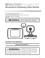
SNUGGLE NEST
Brand: BABY DELIGHT Pages: 12

BC-2200
Brand: Baby Control Pages: 12
View
Brand: iHealth Pages: 12

d10
Brand: Racegeek Pages: 3

MultiRAE
Brand: Rae Pages: 4

UN32C5000QF
Brand: Samsung Pages: 139

SyncMaster 933HD Plus
Brand: Samsung Pages: 43

SyncMaster S19C200BR
Brand: Samsung Pages: 112

SyncMaster S24C200BL
Brand: Samsung Pages: 106

SyncMaster 460DR
Brand: Samsung Pages: 25

P2250W
Brand: Samsung Pages: 41
X246
Brand: Sceptre Pages: 32

babiDolce
Brand: ItsImagical Pages: 16

d10
Brand: Racegeek Pages: 23

YUR.VISION YV216WB1
Brand: YURAKU Pages: 2

MP101M
Brand: Environnement Pages: 196

HJA-313
Brand: Omron Pages: 36

Q72B - Optiquest - 17" LCD Monitor
Brand: ViewSonic Pages: 2


