background image

1-4

Fig. 3

SAFETY CHECK AFTER SERVICING

Examine the area surrounding the repaired location for damage or deterioration. Observe that screws, parts and
wires have been returned to original positions. Afterwards, perform the following tests and confirm the specified
values in order to verify compliance with safety standards.

• Insulation resistance test

confirm the specified insulation resistance or greater between power cord plug prongs and externally exposed
parts of the set (RF terminals, antenna terminals, video and audio input and output terminals, incrophone jacks, 
earphone jacks, etc.) See table below.

• Dielectric strength test

Confirm specified dielectric strength or greater between power cord prongs and exposed accessible parts of
the set  (RF terminals, antenna terminals, video and
audio input and output terminals, incrophone jacks,
earphone jacks, etc.) See table below.

• Clearance distance

When replacing primary circuit components, confirm
specified clearance distance (d), (d') between sol-
dered terminals, and between terminals and sur-
rounding metallic parts. See table below.

Table 1 : Ratings for selected areas

* Class II model only.

Note. This table is unofficial and for reference only. Be sure to confirm the precise values for your particular 

country and locality.

• Leakage Current test

Confirm specified or lower leakage current between B(earth ground, power cord plug prongs) and externally 
exposed accessible parts (RF terminals, antenna terminals, video and audio input and output terminals, micro-
phone jacks, earphone jacks, etc.)

Measuring Method: (Power ON)
Insert load Z between B(earth ground, power cord 
plug prongs) and exposed accessible parts. Use an 
AC voltmeter to measure across both terminals of 
load Z. See figure and following table.

Table 2:Leakage current ratings for selected areas.

Note. This table is for IEC member only. Be sure to confirm the precise values for your particular country and

Note. 

locality.

Chassis

d

a

Primary   circuit   terminals

Exposed
accessible
part

Z

Load

AC  Voltmeter

Earth  Ground,
Power  cord  plug  prongs

B

Fig. 2

AC Line Voltage

AC Line Voltage

100 to 130 V

200 to 240 V

*100 to 130 V

*

200 to 240 V

Europe

Australia

Europe

Australia

Other terminals

Antenna earth

terminals

E

0.7m A peak

E

2m A DC

E

0.7m A peak

E

2m A DC

F

10 M

/500 V DC

4kV 1 minute

F

6mm(d)

F

8mm(d)

(a Power cord) 

Region

Load Z

Leakage Current(i)

Earth Ground

(B) to :

Region

Insulation

Resistance

Dielectric

Strength

Clearance

Distance(d),(d)

2k

50k

Summary of Contents for DVP7771

Page 1: ...1 1 CONTENTS SECTION 1 SUMMARY SECTION 2 EXPLODED VIEWS SECTION 3 ELECTRICAL SECTION 4 REPLACEMENT PARTS LIST...

Page 2: ...1 2 SECTION 1 SUMMARY CONTENTS PRODUCT SAFETY SERVICING GUIDELINES FOR VIDEO PRODUCTS 1 3 SAFETY CHECK AFTER SERVICING 1 4 SPECIFICATIONS 1 5...

Page 3: ...YS WHEN THE HIGH VOLTAGE IS AT THE FACTORY SPECIFIED LEVEL THE PROPER VALUE IS GIVEN IN THE APPLICABLE SCHEMATIC OPERA TION AT HIGHER VOLTAGES MAY CAUSE A FAILURE OF THE PIC TURE TUBE OR HIGH VOLTAGE...

Page 4: ...el only Note This table is unofficial and for reference only Be sure to confirm the precise values for your particular country and locality Leakage Current test Confirm specified or lower leakage curr...

Page 5: ...R21 EMC CSA FCC Regional code Refer to DVD VIDEO Specification Book RATING ITEM SPECIFICATIONS POWER REQUIREMENT DC Adaptor 9 8V Battery 8 0V POWER CONSUMPTION 10W With Battery OPERATING TEMPERATURE R...

Page 6: ...2 1 SECTION 2 EXPLODED VIEWS CONTENTS EXPLODED VIEWS 2 2 Cabinet and Main Frame Section 2 2 Deck Mechanism Section 2 3 Packing Accessory Section 2 4...

Page 7: ...ion 270 A46 451 271 451 290 268 260 261 262 264 269 267 266 263 251 250 278 451 279 254 255 252 253 257 258 256 272 A49 276 273 274 275 452 286 452 280 A47 282 265 284 283 287 281 285 A48 451 A43A A44...

Page 8: ...2 3 Deck Mechanism Section 430 430 001 430 002 002 006 005 004 003 002 431 431 007...

Page 9: ...sory Section PACKING SHEET 804 PACKING OPTIONAL PARTS 803 OWNER S MANUAL 801 REMOCON 900 R C BATTERY 808 BOX CARTONX 802 PACKING 803 812 830 PLUG ASS Y 2WAY ADAPTER 814 PLUG ASS Y 813 S VHS CABLE BATT...

Page 10: ...3 1 SECTION 3 ELECTRICAL CONTENTS LCD PART 3 2 ELECTRICAL TROUBLE SHOOTING GUIDE 3 17 BLCOK DIAGRAMS 3 26 CIRCUIT DIAGRAM 3 32 PRINTED CIRCUIT DIAGRAMS 3 62...

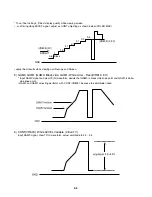
Page 11: ...orm and VR815 adjust with 63 5us center in display 3 RGB AMP adjusting Black Level adjusting Fixed Input RAMP or 5STEP signal TP G waveform adjust while viewing Adjust between 0 5V 4 5V 4 BRIGHT adjus...

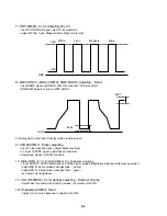
Page 12: ...AM1 GAM0 Black side GAM1 White side Fixed VR810 811 Input RAMP signal and view TP G waveform deside that GAM0 is black side knee point and GAM1 iswhite side knee point GAM0 and GAM1 adjusting performs...

Page 13: ...ck maximum or Input 10 STEP signal adjust Black maximum Adjust best signal in ZOOM condition 10 WB B VR807 2 1V WB R VR806 2 3V Brighness adjusting Input 5STEP 10STEP and Black and White signal adjust...

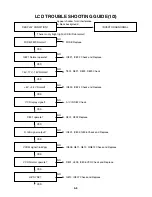
Page 14: ...S W Check X801 C832 Replace IC801 IC803 Q806 Check and Replace IC808 Q811 Q812 QQ813 Check and Replace D801 L809 IC806 VCO Check and Replace Q810 IC807 Check and Replace FUSE F801 Normal Q8F1 Normal o...

Page 15: ...ion TFT LCD pressure voltage 17V 15V 5V 3 3V Power source and D803 D804 Check TFT LCD Normal Replace Color Adjusting Normal Readjust as adjustement standard Each CONNECTOR Replace and Reassemble INVER...

Page 16: ...3 7 LCD BLOCK DIAGRAM CON 8 0 3 INVERTER TFT LCD CROMA IC IR3Y29BM CONTROL IC MN5814 POWER LCD MODE CONTROL Y C COMPOSITE DC9V AC550V SYNC SEP VCO H V R G B CONTROL 3 3V 5V 7 5V 17V 15V...

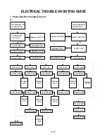
Page 17: ...e ADAPTOR NO 1 8V Is Q109 OK NO 12V NO 5V NO 3 3V NO LCD POWER Replace Q109 Is E 5V OK Is Q112 OK Is Q113 OK Replace Q110 Replace Q112 Replace Q113 Is Q108 OK Replace Q108 Is Q106 OK Replace Q106 Repl...

Page 18: ...W Check Video signals from MPEG Check TR Buffer Q471 Q472 Q473 Check LC Filter AUDIO IN SPEAKER ABNORMAL Check Audio Jack Mode S W Is Q481 OK VIDEO IN ABNORMAL Check Video Jack Mode S W Is IC461 OK Ch...

Page 19: ...If OK Replace B D PICTURE ABNORMAL Check Disc YES If OK YES If OK Refer to Servo part Replace B D DISC ERROR Check the connection of CON 901 Check IC303 Pins 89 82 YES NO NO YES YES If OK YES Reconnec...

Page 20: ...oder Does the moving picture of the video CD play on the screen normally Does the audio sound output normally END Check power clock Check CD DVD DSP output signal Check MPEG Decoder input signal Check...

Page 21: ...710 R711 Solder defective parts again T701 Check the connection of CON901 CON701 Check waveform of IC701 Pin46 47 Does pulse waveform of RC901 Pin 1 appear Is IC701 Pin 49 connected to RC901Pin1 Is RC...

Page 22: ...o IC207 Pin59 Replace IC207 Check power circuit Replace X201 or IC211 33 8688MHz clock defect CHECK POINT General Is IC203 Pin79 80 84 88 about 2 2V END NO NO NO NO NO YES YES YES YES YES Does signal...

Page 23: ...s move up and down Check Focus Driver output IC207 Pin 88 IC2M1 Pins 13 14 Check SLED Driver output IC201 Pin 80 IC2M1 Pin15 16 IC207 Pin 80 no output IC207 is defective IC2M1 Pin 15 no output IC2M1 i...

Page 24: ...n appear OPEN CLOSE Replace COM or IC201 Replace IC207 Check IC2A1 Pin 11 12 13 14 in DVD Mode Fig 3 FOCUS ERROR waveform IC201 no output Pick up is defective Check IC207 and IC2M1 when CON203 Pin3 is...

Page 25: ...rn RF 1 5 1 6V IC2A1 Pin 57 Fig 5 RF waveform Check IC2A1 Pins 5 6 7 8 No signal Pick up is defective Replace IC207 Check IC207 Pin84 No signal at IC207 IC207 is defective Check IC207 Pin 165 Check th...

Page 26: ...T S Drive CD DVD Decoder Servo RF IC SDRAM Battery DC DC Converter Builten BATT Charger System Power Supply Power Control AC Adapter Spindle Drive SDARM FLASH CPU MPEG Deconder TV Enconder Tuner LCD P...

Page 27: ...CON CON902 7 2V LOAD S W Q109 SI3863 DC DC CON IC104 MAX1744 DC DC CON IC108 MAX1775 DC DC CON IC109 MAX1605 FET Q106 SI9407 FET Q107 SI9939 FET Q108 SI1403 5V LOAD S W Q110 SI3865 LOAD S W Q113 SI38...

Page 28: ...sled Spindle M D PICK UP MCK IC 207 HDC25D811 CD DVD DSP DVD SERVO IC2A1 3 3 3P3721 RF Signal Processor FDO TDO FMO UCOM I F DVD A B C D FE TE PI SBADD 4 DVD CD RF DRAM 256K x 16bit 16 9 ICADDR 0 8 IC...

Page 29: ...udio DAC SPEAKER LEFT L J405 EARPHONE JACK DA_LRCK AOUT3 DA_BCK PCMCLK R IC402 NJM4580 OP AMP R L IC413 NJM4580 OP AMP L R IC403 NJU4052 ANALOG MUX IC414 BA7786 SPEAKER EARPHONE AMP J404 Audio I O Jac...

Page 30: ...3 30 IC303 XC9572XL CPLD IC501 PANTERA2 _LE LC FILTER LC FILTER LC FILTER IC461 NJM2233 BUFFER BUFFER BUFFER LCD BOARD CVBS C Y VIDEO_IO_CON LCD 1 5 CVBS I O JACK S VIDEO JACK 5 VIDEO BLOCK DIAGRAM...

Page 31: ...SQS0 SDCLK1 PSYNC DSP_INT SENSE DSP_CS AD 00 20 RF MOTOR I F MIRR LDON SCLK SD ATA EE_CS F_IN 32 MD 00 31 MCLK2 CKE MA 00 10 MA12 13 CS0 RAS CAS WE DQM 0 3 SPINDLE_FG ALE AD 04 19 16 LADD 04 19 16 LA...

Page 32: ...MEMO...

Page 33: ...3 8 3 9 LCD CIRCUIT DIAGRAM LCD1 CIRCUIT DIAGRAM No power No power No power No power Not operate 5V 3 3V Line dead 3 3V Line dead 2002 02 01 R14121A...

Page 34: ...D2 CIRCUIT DIAGRAM Display abnormal Black Display abnormal unstable Color abnormal Color abnormal No display Side black abnormal Speaker 1 Dimmig abnormal No Display Black background Speaker 2 2002 02...

Page 35: ...3 12 3 13 LCD3 CIRCUIT DIAGRAM Display unstable Display unstable brightness abnormal Interface Line occur Vcom abnormal Display abnormal 2002 02 01 R14120A...

Page 36: ...3 C SYNC 36 2 4 Y signal 0 5 37 2 1 38 4 7 COM 3 4 7 39 0 40 2 41 2 42 2 43 5 VCC 44 1 3 45 2 7 46 2 9 47 3 2 48 2 7 PIN NO VOLT WAVEFORM 1 0 2 3 3 HD 0 3 3 3 0 4 0 5 3 3 VD 0 3 3 6 2 8 HQ OUT 7 2 8...

Page 37: ...3 15 3 16 LCD P C BOARD LOCATION GUIDE LOCATION GUIDE...

Page 38: ...MEMO MEMO...

Page 39: ...defective E 5V is bad Q101 is defective 1 8V 3 3 ard bad IC108 is defective 1 8V 3 3V are bad IC109 is defective 12V is bad Q107 is defective 3 3V is bad Q108 is defective 12V is bad IC120 is defectiv...

Page 40: ...3 34 3 35 2 DRIVER CIRCUIT DIAGRAM Sled Not mone Tracking Sled Spindle Focuse waveforms page 3 58 3 59 2002 02 01 R14109A...

Page 41: ...3 36 3 37 3 RF CIRCUIT DIAGRAM CD DVD LD abnormal CD DVD picture abnomal DVD LD abnormal DVD LD abnormal Tracking Focuse waveforms page 3 58 3 59 2002 02 01 R14110A...

Page 42: ...3 38 3 39 4 DSP CIRCUIT DIAGRAM Focus Servo Fail Tracking Servo Fail Sled Servo Fail Spindle Motor abnormal DRAM control MPEG Signal Tracking Sled Spindle Focuse 2002 02 01 R14111A...

Page 43: ...RAM CIRCUIT DIAGRAM Q2A2 are defective CD LD will not be on Q2A1 are defective DVD LD will not be on Q2A3 are defective NO focus Arocking Control IC 212 is defective Scratched LD audio abnormal 2002 0...

Page 44: ...3 42 3 43 6 PANTER CIRCUIT DIAGRAM waveforms page 3 58 3 59 2002 02 01 R14113A...

Page 45: ...3 44 3 45 7 MEMORY CIRCUIT DIAGRAM 2002 02 01 R14114A...

Page 46: ...3 46 3 47 8 X BUS CIRCUIT DIAGRAM Q501 is defective Key S W voltage abnormal 2002 02 01 R14115A...

Page 47: ...3 48 3 49 9 CPLD CIRCUIT DIAGRAM 2002 02 01 R14116A...

Page 48: ...3 50 3 51 10 VIDEO CIRCUIT DIAGRAM Q472 is defective C signal is bad Q471 is defective Y signal is bad COMP Video S Video Y S Video C 2002 02 01 R14117A...

Page 49: ...Audio Out Bad IC413 is defective ICH Audio IC403 is defective 2CH Audio out is bad IC414 is defective speakers earphone are bad Q406 is defective Optical out is bad IC401 is defective 2CH Audio out ba...

Page 50: ...3 54 3 55 12 FRONT CIRCUIT DIAGRAM System not operate System not operate Power not control Q701 is defective key S W voltage abnormal 2002 02 01 R14122A...

Page 51: ...3 56 3 57 13 REMOCON CIRCUIT DIAGRAM Remocon not operate Q902 is defective LED not operate 2002 02 01 R14123A...

Page 52: ...s Search Case IC501 Pin 112 Chrominance Super video out Mode IC501 Pin 114 Luminance Super video out Mode IC501 Pin 99 MPEG Clock 27MHz CH1 IC2A1 Pin42 Focus Error CH2 IC2M1 Pin21 Focus Drive Disc Det...

Page 53: ...7 3 13 3 10 19 5 5 37 2 56 1 84 4 9 60 9 55 88 2 17 2 16 88 3 14 3 10 20 2 514 2 51 38 0 00 0 00 89 1 97 1 97 89 1 80 1 80 21 2 514 2 51 39 2 40 2 76 Q109 Q109 Q109 Q109 90 1 61 1 61 90 0 00 3 10 22 0...

Page 54: ...3 62 3 63 PRINTED CIRCUIT DIAGRAMS 1 MAIN P C BOARD LOCATION GUIDE LOCATION GUIDE...

Page 55: ...3 64 3 65 2 FRONT KEY P C BOARD LOCATION GUIDE LOCATION GUIDE...

Page 56: ...MEMO MEMO...

Reviews: