background image

16

UB99

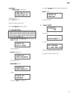
3-1-19. VR Check

Turn VR3 (Control 3) slightly clockwise.  The following

display appears.

Check for the OK sign in the display.

3-1-20. USB Check

Push [ON/OFF] SW.  The following display appears.

3-1-21. USB Check

Connect with PC by USB cable.  The following display

appears.

3-1-22. USB Check

Remove the USB cable.  The following display appears.

Check for the OK sign in the display.

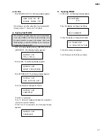
3-1-23. LCD Check

Push [ON/OFF] SW.  The following display appears.

3-1-24. LCD Check

Push [ON/OFF] SW.  The following display appears.

All the LEDs will be turned on.

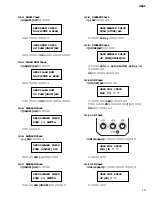
3-1-13. VR Check

Turn VR1 (Control 1) slightly clockwise.  The following

display appears.

3-1-14. VR Check

Turn VR2 (Control 2) fully clockwise.  The following

display appears.

3-1-15. VR Check

Turn VR2 (Control 2) fully counterclockwise.  The

following display appears.

3-1-16. VR Check

Turn VR2 (Control 2) slightly clockwise.  The following

display appears.

3-1-17. VR Check

Turn VR3 (Control 3) fully clockwise.  The following

display appears.

3-1-18. VR Check

Turn VR3 (Control 3) fully counterclockwise.  The

following display appears.

UB99   VOL2   CHECK

MAX   **   [**]   **

UB99   VOL2   CHECK

MIN   **   [ff ]   **

UB99   VOL2   CHECK

UP   **   [00]   **

UB99   VOL3   CHECK

MAX   **   **   [**]

UB99   VOL3   CHECK

MIN   **   **   [ff]

UB99   VOL3   CHECK

UP   **   **   [00]

UB99   VOL3   CHECK

OK   PUSH [ONOFF] SW

UB99   USB   CHECK

V10103   CNECT   USB

UB99   USB   CHECK

DISCONNECT   CABLE

UB99   USB   CHECK

OK   PUSH [ONOFF] SW

UB99   LCD   CHECK

PUSH   [ON/OFF]   SW

■■■■■■■■■■■■

■■■■■■■■■■■■

Summary of Contents for Magicstomp UB99

Page 1: ...T 4 BLOCK DIAGRAM 5 CIRCUIT BOARD LAYOUT 6 DISASSEMBLY PROCEDURE 6 LSI PIN DESCRIPTION 8 IC BLOCK DIAGRAM 11 CIRCUIT BOARD 12 INSPECTIONS FACTORY SET 14 18 BACKUP THE USER PATCH DATA 22 ERROR MESSAGES 23 PARTS LIST CIRCUIT DIAGRAM GUITAR EFFECTS PROCESSOR UB99 目次 総合仕様 パネルレイアウト ブロックダイアグラム ユニットレイアウト 分解手順 LSI端子機能表 ICブロック図 シート基板図 検査 ファクトリーセット ユーザーパッチのバックアップ エラーメッセージ 回路図 ...

Page 2: ...d failure of the product to perform as specified For these reasons we advise all Yamaha product owners that all service required should be performed by an authorized Yamaha Retailer or the appointed service representative IMPORTANT This presentation or sale of this manual to any individual or firm does not constitute authorization certifi cation recognition of any applicable technical capabilities...

Page 3: ... MONO R 0dBm 1 kΩ Power Exclusive Power Adaptor AC 10 AC Output AC 12 V 1 A Power Consumption 12 W Dimensions W x H x D 164 x 62 x 176 mm 6 7 16 x 2 7 16 x 6 15 16 Weight 910 g 2lbs Accessories Power Adaptor AC 10 CD ROM USB Cable Owner s Manual Patch List 総合仕様 デジタル部 デジタルシグナルプロセッシング エフェクター 専用エディターソフト Sound Editor for MAGICSTOMP 同梱 パッチセレクト 2モード クロマチックオートチューナー内蔵 通信機能 受信 Parameter Change Bulk In 1 pa...

Page 4: ...Switch Switch ON OFF Switch y INPUT Jack u INPUT LEVEL HIGH LOW Switch i OUTPUT L MONO R Jacks o USB Jack 0 AC IN Jack Power Adaptor Top Panel Rear Panel パネルレイアウト ディスプレイ コントロールツマミ ボリュームツマミ ストアボタン スイッチ スイッチ ON OFF スイッチ インプット端子 インプットレベル切替スイッチ アウトプット端子 USB 端子 電源アダプター端子 トップパネル リアパネル ...

Page 5: ...IC102 8P IC104 28P IC105 8P IC106 8P IC7 64P IC4 100P IC1 48P SYSTEM RESET IC2 28P IC10 44P IC6 44P D106 112 TR105 106 IC5 176P 2 3 4 5 19 15 13 14 12 4 63 66 67 55 65 3 28 27 26 25 IC103 8P IC3 5P JK102 JK103 CN1 JK104 AC 10 X3 X2 X1 IC111 IC109 IC108 IC112 IC113 12 13 ブロックダイアグラム ...

Page 6: ...nd the two 2 screws marked 30 The bottom case can then be removed Fig 1 1 ボトムケース 所要時間 約 1 分 1 1 40 のネジ4本と 30 のネジ2本を外し ボトムケー スを外します 図 1 40 40 30 Bottom case ボトムケース 30 Bind Head Tapping Screw B 3 0X8 MFZN2BL EP600190 40 Bind Head Tapping Screw P 4 0X8 MFZN2BL VB931600 Fig 1 DM Bottom view Bottom view ユニットレイアウト 分解手順 バインドBタイト バインドPタイト 図1 ...

Page 7: ...ます 1 項参照 2 2 リアパネル面より 110 のネジ2 本と 120 の特殊六 角ナット 3 個 130 の特殊平座金 3 個を外し AC コードコラムとリアパネルを外します 図 2 4 Foot Switch Time required About 3 minutes 4 1 Remove the bottom case See Procedure 1 4 2 Remove the rear panel See Procedure 2 4 3 Remove the DM circuit board See Procedure 3 4 4 Remove the hexagonal nut of the foot switch The foot switch can then be removed Fig 2 Photo 1 4 フットスイッチ 所要時間 約 3 分 4 1 ボトムケー...

Page 8: ...1 82 83 84 85 86 87 88 89 90 91 92 93 94 95 96 97 98 99 100 P26 A14 P27 A15 P50 A16 P51 A17 P52 A18 P53 A19 VSS P60 WAIT P61 BREO P62 BACK P67 STBY RES NMI VSS EXTAL XTAL VCC P63 AS P64 RD P65 HWR P66 LWR MD0 MD1 MD2 AVCC VREF AN0 P70 AN1 P71 AN2 P72 AN3 P73 AN4 P74 AN5 P75 DA0 AN6 P76 DA1 AN7 P77 AVSS IRQ0 P80 CS3 IRQ1 P81 CS2 IRQ2 P82 ADTRG CS1 IRQ3 P83 CS0 P84 VSS TCLKA TP0 PA0 TCLKB TP1 PA1 TC...

Page 9: ... AN2 P13 DQ3 AN3 P14 DQ4 AN4 P15 DQ5 AN5 P16 DQ6 AN6 P17 DQ7 AN7 CNVSS RESET VCCE VREF VSS XIN VOUT VCC CNVSS2 P60 LED0 P61 LED1 P62 LED2 P63 LED3 PVSS PVCC DVCC USBVREF TrON D0 D0 P20 P21 P22 P23 P24 P25 I O I O I O I O I O I O I I I I O I I O I O I O I O O I O I O I O I O I O I O I O I O Port P1 In output Chip active System reset input Analog power supply 3 3V Reference voltage input Ground Cloc...

Page 10: ...5 V Data bus of internal register WAIT output Ground Serial data input Ground Power supply 5 V Serial data output Ground Parallel data bus Power supply 5 V Power supply 3 3 V 89 90 91 92 93 94 95 96 97 98 99 100 101 102 103 104 105 106 107 108 109 110 111 112 113 114 115 116 117 118 119 120 121 122 123 124 125 126 127 128 129 130 131 132 133 134 135 136 137 138 139 140 141 142 143 144 145 146 147 ...

Page 11: ...Dual Operational Amplifier DM IC102 103 105 106 R T R T R T R T R T R T R T R T R T R T R T R T 9 5 3 2 4 13 12 14 15 1 11 10 CLR CLK QA QD QE QH QK QL QF QG QI QJ 7 QB 6 QC 1 2 3 4 5 6 7 1A 1Y 2A 2Y 3A 3Y Vss 14 13 12 11 10 9 8 VDD 6A 6Y 5A 5Y 4A 4Y 1 2 3 4 5 6 7 20 19 18 17 16 15 14 Vcc G B1 B2 B3 B4 B5 B6 B7 B8 8 9 10 12 11 GND A8 A7 A6 A5 A4 A3 A2 A1 D1R 13 Output A Inverting Input A Non Inver...

Page 12: ...CUIT BOARD INPUT R OUTPUT L MONO USB AC IN INPUT LEVEL HIGH LOW DM Circuit Board CNA WC10200 2 1 Component side 部品側 Note See parts list for details of circuit board component parts シート基板図 注 シートの部品詳細はパーツリストをご参照ください ...

Page 13: ...UB99 13 CONTROL 1 CONTROL 2 STORE CONTROL 3 VOLUME ON OFF ON OFF DM Circuit Board CNA WC10200 3 Pattern side パターン側 ...

Page 14: ... you will get TEST MODE Proceed with inspection according to the instruction in the following display Make sure that the back light SED of LCD is lit INSPECTIONS FACTORY SET UB99 P CHEK V1 0 PUSH ON OFF SW 3 1 1 DSP DRAM AD DA Check Push ON OFF SW The following display appears Make sure that a signal wave is outputted 3 1 2 Electrical characteristics U B99 DSP DRAM PUSH ON OFF SW Item Input termin...

Page 15: ... display is changed as follows Check for the OK sign in the display 3 1 4 FLASH ROM Check Push ON OFF SW The following display appears In a short time the display is changed as follows Check for the OK sign in the display 3 1 5 SW LED Check Push ON OFF SW The following display appears Check for the OK sign in the display 3 1 6 SW LED Check Push SW The following display appears and LED will be turn...

Page 16: ...1 slightly clockwise The following display appears 3 1 14 VR Check Turn VR2 Control 2 fully clockwise The following display appears 3 1 15 VR Check Turn VR2 Control 2 fully counterclockwise The following display appears 3 1 16 VR Check Turn VR2 Control 2 slightly clockwise The following display appears 3 1 17 VR Check Turn VR3 Control 3 fully clockwise The following display appears 3 1 18 VR Check...

Page 17: ...atch contents you saved are erased Take notes of the settings or save the settings on your computer if necessary See page 22 Turn on power while pushing ON OFF SW and STORE SW The following display appears Push SW The following display appears Push STORE SW The following display appears Then the display is changed as follows The SET is completed Then 5 Opening display will appear and operation ret...

Page 18: ... LCDバックライトLEDが点灯していることを確認します UB99 P CHEK V1 0 PUSH ON OFF SW 3 1 1 DSP DRAM AD DA Check ON OFF SW を押します と表示され 信号波形が出力されるのを確認します 3 1 2 電気的特性 UB99 DSP DRAM PUSH ON OFF SW 項目 入力端子 条件 出力端子 規格値 1 入力感度 INPUT OUT L MONO 4 5dBm 1KHz 0dBm 3dB 2 同上 INPUT OUT L MONO 4 5dBm 10KHz 0dBm 3dB 3 同上 INPUT OUT L MONO 4 5dBm 100Hz 0dBm 3dB 4 同上 INPUT OUT R 22 5dBm 100Hz 0dBm 3dB 5 同上 INPUT OUT R 22 5dBm 10KHz 0dBm 3d...

Page 19: ...D UB99 FLASH ROM OK PUSH ONOFF SW UB99 SW LED CHECK PUSH SWITCH UB99 SW LED CHECK PUSH ON OFF SW UB99 SW LED CHECK PUSH SWITCH 3 1 8 SW LED Check SW を押します と表示され LED が点灯します 3 1 9 SW LED Check STORE SW を押します と表示され LED LED ON OFF LED が 3 個点灯します OK 表示を確認してください 3 1 10 VR Check ON OFF SW を押します と表示されます LED は消灯します はそれぞれの VR の値を表示します が検査する VR の位置を示します 3 1 11 VR Check VR1 Control 1 を右にいっぱいまで回します と表示されます 3 1...

Page 20: ...CK MIN ff UB99 VOL2 CHECK UP 00 UB99 VOL3 CHECK MAX UB99 VOL3 CHECK MIN ff UB99 VOL3 CHECK UP 00 3 1 19 VR Check VR3 Control 3 を右に少し回します と表示されます OK 表示を確認してください 3 1 20 USB Check ON OFF SW を押します と表示されます 3 1 21 USB Check USB Cable で P C と接続します と表示されます 3 1 22 USB Check USB Cable を抜きます と表示されます OK 表示を確認してください 3 1 23 LCD Check ON OFF SW を押します と表示されます 3 1 24 LCD Check ON OFF SW を押します と全点灯されます UB99 VOL3 CH...

Page 21: ...F SW と STORE SW を押しながら電源を ON にします と表示されます SW を押します と表示されます STORE SW を押すと となり と表示され SET が完了します UB99 DIAG ALL OK PLEASE POWER OFF FACTORY SET NO YES FACTORY SET SURE PUSH STORE FACTORY SET NOW FACTORY SET FACTORY SET COMPLETE FACTORY SET CANCELLED その後5 Opening 表示をし通常動作となります Cancel の時は と表示されます 5 Opening MODE と表示され と変わり となります この画面は参考例です 電源を切って終了してください MAGICSTOMP V1 01 WAIT A MOMENT U01 TUBE DRIVE GAIN...

Page 22: ...emory are transferred to the computer The MAGICSTOMP s display will indicate how much data has been transferred 5 MAGICSTOMPのユーザーパッチの内容がコンピュー ターに送られます MAGICSTOMP のディスプレイに は パッチデータの送信状況が表示されます BACKUP THE USER PATCH DATA Bulk Transmit Button バルク受信ボタン 6 The Bulk Receive operation is complete when the contents of the MAGICSTOMP s User Patch memory appears in the library window 7 Click on the Close but...

Page 23: ...Check the USB cable connection computer settings etc An error occurred while transmitting or receiving bulk data Check the USB cable con nection Also if the error occurs about halfway through the operation setting the inter val speed to a slower setting sometimes solves the problem The hardware is damaged MAGICSTOMPにエラーが発生した場合 ディスプレイに次のエラーメッセージが表示されます 操作を一時中断し それ ぞれの対処方法に従ってください バルクアウトしようとしたデータが壊れ...

Page 24: ...r is O not zero The second letter of the shaded part number is I not one M South African model O Chinese model Q South east Asia model T Taiwan model U U S A model V General export model 110V W General export model 220V N X General export model Y Export model A Australian model B British model C Canadian model D German model E European model F French model H North European model I Indonesian model...

Page 25: ... AC Adaptor AC 10 J J 08 AC Adaptor AC 10 U C U C 08 AC Adaptor AC 10 H H 08 CD ROM CD ROM 12cm 4A78 USB Cable 4P 1 5m USB A B WB844900 EP600190 VB931600 WB845100 WB845200 V5882800 V5883000 V5883100 X4770A00 WB930000 OVERALL ASSEMBLY 10 20 30 40 50 50 60 60 Top case assembly See page 3 トップケースAss y AC Output Power Adaptor AC 10 J 部 品 名 総 組 立 トップケースAss y ボ ト ム ケ ー ス バ イ ン ド B タ イ ト バ イ ン ド P タ イ ト レ...

Page 26: ...rew 3 0X8 MFZN2BL 2 01 120 Hexagonal Nut 9 0 12X2 MFNI33 3 01 130 Flat Washer 9 0X14X0 5 MFNI33 3 01 140 Toothed Lock Washer A 9 0 MFZN2Y 3 01 150 AC Cord Column WB842400 WB845300 WB845800 WB842500 WB842900 ET500230 WC102000 WB845700 EP630220 WB845900 VA295800 LX200060 VL802300 ET800150 WC497400 部 品 名 トップケースAss y ト ッ プ ケ ー ス パ ネ ル シ ー ト フ ッ ト ス イ ッ チ パ ネ ル フ ッ ト ス イ ッ チ バ ネ 座 金 特 種 平 座 金 D M シ ー ト...

Page 27: ...01 0125 Ceramic Capacitor F chip 0 1000 25V Z 01 C0126 Ceramic Capacitor SL chip 470P 50V J 01 C0127 Ceramic Capacitor SL chip 470P 50V J 01 C0128 Ceramic Capacitor B chip 3300P 50V K 01 C0129 Electrolytic Cap NK 10 00 25 0V 01 C0130 Electrolytic Cap 10 00 25 0V 01 C0131 Ceramic Capacitor CH chip 22P 50V J 01 C0132 Electrolytic Cap NK 10 00 25 0V 01 C0133 Electrolytic Cap NK 10 00 25 0V 01 C0134 C...

Page 28: ...0T IC002 IC CY62256VLL 70ZCT IC003 IC S 80128BNMC JGN SYSTEM RESET 01 IC004 IC HD6413008VF25 CPU MAIN IC005 IC YSS910 S DSP6 10 IC005 IC YSS910 V 09 IC006 IC MSM51V4265E 60TS K DRAM 4M 05 IC006 IC GLT440L16 40TC 05 IC007 IC M38K07M4L 303HP CPU USB 10 IC008 IC SN74LV245APWR TRANSCEIVER IC009 IC SN74LV245APWR TRANSCEIVER IC010 IC MSM51V4265E 60TS K DRAM 4M 05 IC010 IC GLT440L16 40TC 05 IC101 IC NJM0...

Page 29: ...1 0080 Carbon Resistor chip 0 0 0 0 J 01 R0081 Carbon Resistor chip 100 0 63M J 01 R0082 Carbon Resistor chip 100 0 63M J 01 R0101 Carbon Resistor chip 10 0K 63M J 01 R0102 Carbon Resistor chip 1 0M 63M J 01 R0103 Carbon Resistor chip 4 7K 63M J 01 R0104 Carbon Resistor chip 4 7K 63M J 01 R0105 Carbon Resistor chip 22 0K 63M J 01 R0106 Carbon Resistor chip 12 0K 63M J 01 R0107 Carbon Resistor chip...

Page 30: ...3 Carbon Resistor chip 10 0K 63M J 01 R0174 Carbon Resistor chip 470 0 63M J 01 R0175 Carbon Resistor chip 10 0K 63M J 01 R0176 Metal Oxide Film Resistor 68 0 1W J 01 R0177 Metal Oxide Film Resistor 68 0 1W J 01 R0178 Metal Oxide Film Resistor 27 0 2W J 01 RA001 Resistor Array 10KX4 01 010 Resistor Array 10KX4 01 SW001 Tact Switch TC 12ED SW002 Tact Switch TC 12ED ON OFF SW003 Tact Switch TC 12ED ...

Page 31: ...rtz Crystal Unit 16 0MHz HC 49SMD X0003 Quartz Crystal Unit 6 0MHz HC 49SMD X0101 Quartz Crystal Unit 22 5792MHz HC 49SMD ZD101 Zener Diode HZU2 0B 2 0V ZD102 Zener Diode HZU2 0B 2 0V ZD103 Zener Diode UDZS 15B TE 17 ZD104 Zener Diode UDZS 15B TE 17 WB445700 WB445700 WB446200 WA692500 WC402600 WC402500 WC402400 V9242500 V9242500 WC165500 WC165500 ロ ー タ リ ー V R ロ ー タ リ ー V R 二 連 ロ ー タ リ ー V R 水 晶 発...

Page 32: ...tes the location of the counter inter sheet connector The alphabet indicates horizontal direction and the number indicates vertical direction to page 1 G4 Signal name 信号名 FLASH ROM 16M PROGRAM SYSTEM RESET CPU MAIN DRAM 4M DSP 6 CPU USB DRAM 4M TRANSCEIVER TRANSCEIVER SRAM 256K to Page 1 G4 to Page 2 H3 from Page 2 C5 from Page 2 F5 from Page 2 G3 to Page 2 G4 from Page 1 D3 from Page 2 H3 Ceramic...

Page 33: ...tal Oxide Film Resistor 酸化金属被膜抵抗 酸金 1SR154 400 VT532500 DIODE DM D106 112 1 ANODE 2 CATHODE 2 1 NJM7915FA XD854A00 REGULATOR 15V DM IC113 1 2 3 1 OUTPUT 2 INPUT 3 COMMON Carbon Resistor chip チップ抵抗 金被1 16W NJM7815FA XD853A00 REGULATOR 15V DM IC112 1 2 3 1 OUTPUT 2 COMMON 3 INPUT NJM78M05DLA XS534A00 REGULATOR 5V DM IC108 109 1 INPUT 2 GND 3 OUTPUT 1 2 3 µPC29M33T E1 XU965A00 REGULATOR 3 3V DM IC111...

Reviews: