background image

EMX66M

EMX66M

EMX66M

A

B

C

D

E

F

G

H

1

2

3

4

5

EMX66M

<P.3>

OP AMP

OP AMP

OP AMP

OP AMP

OP AMP

OP AMP

OP AMP

LED DRIVER

LED DRIVER

OP AMP

(to P.1 G-1)

(to P.2 G-1)

(From P.5 G-4)

(From P.5 G-4)

(to P.4 B-2)
(to P.4 B-3)

(From P.4 E-1)

(From P.5 G-4)

(From P.5 G-5)

(to P.1 G-5)

(to P.2 G-5)

(From P.4 G-5)

(From P.2 G-4)

(From P.1 G-4)

(From P.4 G-5)

(From P.2 G-4)

(From P.1 G-4)

38CC1-8822115-4  1

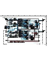
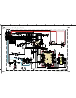
 EMX66M OVERALL CIRCUIT DIAGRAM 3/7 (MIX66 3/5)

Summary of Contents for EMX66M

Page 1: ...D LAYOUT WIRING 10 DIMENSIONS 11 BLOCK LEVEL DIAGRAM 12 DISASSEMBLY PROCEDURE 14 LSI PIN DESCRIPTION 20 IC BLOCK DIAGRAM 22 CIRCUIT BOARDS 23 INSPECTION 33 OVERALL CIRCUIT DIAGRAM PARTS LIST EMX66M Th...

Page 2: ...g disassembly and parts replacement Recheck all work before you apply power to the unit WARNING CHEMICAL CONTENT NOTICE The solder used in the production of this product contains LEAD In addition othe...

Page 3: ...Z to EFFECT OUT CH1 4 48 dB CH IN Low Z to REC OUT CH1 4 56 dB CH IN Hi Z to MAIN OUT MONITOR OUT CH1 4 26 dB AUX IN to MAIN OUT 24 dB 2TR IN to MAIN OUT 66 dB MIC IN to MAIN OUT MONITOR OUT CH5 6 26...

Page 4: ...50 600 Mics 62 dB 0 616 mV 50 dB 2 45 mV 20 dB 77 5 mV XLR 3 31 type2 LINE INPUT CH5 1 2 10 k 600 Lines 22 dB 61 6 mV 10 dB 245 mV 20 dB 7 75 V Phone jack3 Super Hi Z CH6 1 2 470 k 1 k 42 dB 6 16 mV...

Page 5: ...5 EMX66M...

Page 6: ...6 EMX66M...

Page 7: ...FFECT control LEVEL control PAD switch CH1 4 Digital Effect EFFECT select switch ON switch indicator 1 PAD 15 15 1 HIGH MID LOW LEVEL MONITOR EFFECT 15 15 15 15 0 15 0 15 0 10 1 2 3 4 5 DIGITAL EFFECT...

Page 8: ...ch indicator ON OFF switch 10 0 10 0 EFFECT RTN 2TR IN GEQ MASTER 12 6 0 6 12 12 6 0 6 12 125 250 500 1k 2k 4k 8k 6 3 0 5 10 10 0 10 0 MAIN AUX IN 8 9 10 1 1 12 13 10 0 10 0 10 0 EFFECT RTN 2TR IN GEQ...

Page 9: ...rminal INPUT TO MAIN terminal AUX IN 2TR IN OUTPUT terminal REC OUT MAIN MONI TOR SPEAKERS terminal AC IN socket ON OFF power 23 EEEngine SEE REAR PANEL CAUTION Hi Z Hi Z Hi Z Hi Z Low Z Low Z Low Z L...

Page 10: ...05 Power Transformer AC INLET DC Fan POWER ON OFF 1 2 3 4 Location Connector Assembly Remarks Parts No 1 MIX66 PWR1 4 24185 2426 15P L 700 V842620 2 MIX66 DSP 100mm P 1 25 MF12710 3 PWR1 4 PWR2 4 B B4...

Page 11: ...11 EMX66M DIMENSIONS 305mm 481 5mm 448 5mm 327 6mm 62mm Front View Side View Front View with Rack Mount Adaptor...

Page 12: ...1 2 3 1 2 3 4 1 2 3 1 2 3 1 2 3 4 1 2 3 4 1 2 3 4 1 2 3 4 1 2 3 4 1 2 3 4 IC101 301 IC501 IC601 IC603 IC603 IC501 IC502 IC502 IC703 IC703 IC901 IC704 IC704 IC601 IC706 IC306 IC102 302 CN901 27PIN CN9...

Page 13: ...PEAKERS BRIDGE 1 2 A 1 2 B 1 2 3 4 1 2 3 4 1 2 3 4 IC901 IC705 IC805 806 IC705 IC702 IC903 IC903 SW701 SW910 IC802 IC706 IC803 804 CN902 15PIN CN101 15PIN W101RE1 W101BE1 W101RE2 W101BE2 3 1 2 1 3 1 5...

Page 14: ...132700 90 Bind Head Screw 4 0X20 MFZN2BL VB403600 100 Bind Head Screw A4 0X8 MFZN2BL VP156800 Fig 2 2 DSP ZFX Circuit Board Time required about 4 min 2 1 Remove the front panel assembly See Procedure...

Page 15: ...g 5 3 7 Remove the eighteen 18 knobs marked 50 eight 8 knobs marked 60 the nine 9 knobs marked 70 and the eight 8 knobs marked 80 The mix66 circuit board can then be removed Fig 5 Note When placing th...

Page 16: ...g Screw B 4 0X8 MFZN2BL EG340190 60 Bind Head Screw 4 0X12 MFZN2BL VB132700 130 Bind Head Screw 4 0X30 MFZN2BL VT229100 140 Bind Head Tapping Screw B 3 0X12 MFZN2BL VQ074600 150 Bonding Head Tapping S...

Page 17: ...anel assembly See Procedure 5 6 2 Remove the screw marked 150a and the five 5 hexagonal nuts marked C The PWR circuit board 2 4 can then be removed Fig 8 7 PWR Circuit Board 3 4 Time required about 3...

Page 18: ...d 3 4 See Procedure 7 8 4 Remove the sixteen screws marked 90 to remove the TR holder A and the TR holder B Fig 11 8 5 Remove the six 6 screws marked 40 The PWR circuit board 1 4 can then be removed F...

Page 19: ...s former can then be removed Fig 13 Power Transformer FRONT VIEW D 11 Front Frame Time required about 6 min 11 1 Remove the front panel assembly See Procedure 1 11 2 Remove the four 4 screws marked 50...

Page 20: ...trol Input Interrupt 1 Audio Data Receive Unit 1 bit Clock Audio Data Receive Unit 2 bit Clock Audio Data Transmitt Unit 1 Data Output Audio Data Transmitt Unit 2 Data Output Audio Data Transmitt Unit...

Page 21: ...put port Port 3 8 bits input output port Port 3 8 bits input output port Clock output Port 3 8 bits input output port Buzzer output Port 3 8 bits input output port Input only 4 bits input output port...

Page 22: ...JM2060M TE2 OP XM560A00 Quad Operational Amplifier MIX66 IC803 IC804 IC805 IC806 NJM4558MT 1 IG103520 Dual Operational Amplifier NJM2068MD T1 XJ553A00 TL072CPSR XV423A00 1 2 3 4 V 8 7 6 5 Output A V N...

Page 23: ...24 MIX66 CIRCUIT BOARD PATTERN SIDE 26 DSP CIRCUIT BOARD COMPONENT SIDE 28 DSP CIRCUIT BOARD PATTERN SIDE 29 PWR 1 4 CIRCUIT BOARD COMPONENT SIDE 30 PWR 2 4 CIRCUIT BOARD COMPONENT SIDE 32 PWR 3 4 CIR...

Page 24: ...D HIGH MID LOW MONITOR EFFECT LEVEL PAD HIGH MID LOW MONITOR EFFECT LEVEL HIGH MID LOW MONITOR EFFECT LEVEL HIGH MID LOW MONITOR EFFECT LEVEL PAD Hi Z Hi Z Hi Z Hi Z Low Z Low Z Low Z Low Z MIC MIC Su...

Page 25: ...0 YAMAHA SPEAKER PROCESSING POWER AMP MODE PHAMTOM ON OFF MONITOR GRAPHIC EQUALIZER MAIN GRAPHIC EQUALIZER EFFECT RTN EFFECT RTN AUX IN 2TR IN 2TR IN MASTER MASTER ON VOVAL ECHO 1 VOVAL ECHO 2 VOVAL R...

Page 26: ...26 EMX66M A A MIX66 Circuit Board...

Page 27: ...27 EMX66M A A Pattern side 3NA V826690 1...

Page 28: ...28 EMX66M to MIX66 CN901 DSP Circuit Board Component side 3NA V826710 1...

Page 29: ...29 EMX66M Pattern side 3NA V826710 1...

Page 30: ...30 EMX66M to PWR2 4 W101BE2 to PWR to PWR2 4 W101RE2 to PWR1 4 W103OR1 to MIX66 CN902 A A PWR 1 4 Circuit Board...

Page 31: ...31 EMX66M to PWR1 4 W103OR2 to FAN Assembly to Power Tranceformer to PWR2 4 W101BL2 to PWR2 4 W101WH2 A A Component side 3NA V826900 1...

Page 32: ...1 BRIDGE SPEAKERS 1 2 1 2 A B PWR 2 4 Circuit Board Component side AC IN to Power Tranceformer to PWR 4 4 CN107 Component side PWR 3 4 Circuit Board ON OFF to PWR 3 4 W102YE W102BR PWR 4 4 Circuit Boa...

Page 33: ...the load of 10k to MAIN OUT MONITOR OUT EFFECT OUT and REC OUT terminal Set each control as follows CH INPUT 1 4 EQ HIGH MID LOW level control CENTER MONITOR level control MAX EFFECT level control MAX...

Page 34: ...output level does not meet the table change the input frequency until the output level meets the table If the frequency variation is within 20 of the rated value the rusult can be regarded as OK Table...

Page 35: ...is more than the rated value find the noise level converted from the input level for each channel Then confirm that the noise level is less than 124dB as for CH1 5 and less than 122dB as for CH6 2 10...

Page 36: ...NE 1 POWER AMP switch MAIN MAIN OUTPUT terminal SPEAKERS A1 SPEAKERS B1 Load Resistance 4 more than 300W Except otherwise indicated the load resistance should be connected only for the power amplifier...

Page 37: ...e condition as 1 3 Remove the 4 load resistance and connect only 10pF 0 47 F capacitor as load and apply rectangule signal of 10kHz 26dBs Then confirm that the system does not oscillate Besides confir...

Page 38: ...xcept the above same as the setting of 2 1 3 2 2 Gain Check Apply 26 0dB signal into input terminal and confirm that the output level of 22 0 2 dBs can be gained 3 2 3 Frequency Response Check Apply 2...

Page 39: ...39 EMX66M...

Page 40: ...40 EMX66M...

Page 41: ...41 EMX66M...

Page 42: ...42 EMX66M...

Page 43: ...43 EMX66M...

Page 44: ...44 EMX66M...

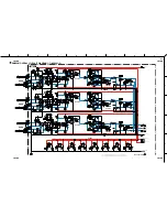
Page 45: ...1 2 3 4 5 EMX66M P 1 EMX66M OVERALL CIRCUIT DIAGRAM 1 7 MIX66 1 5 MIX66 OP AMP OP AMP OP AMP OP AMP OP AMP OP AMP OP AMP From P 3 F 4 to P 3 A 3 to P 4 B 4 to P 3 A 4 From P 3 A 5 From P 5 G 5 From P...

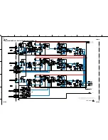
Page 46: ...MX66M EMX66M EMX66M P 2 OP AMP OP AMP OP AMP OP AMP OP AMP OP AMP OP AMP From P 3 F 4 From P 5 G 5 From P 5 G 4 to P 3 A 3 to P 4 B 4 to P 3 A 4 From P 3 A 5 From P 1 G 5 38CC1 8822115 3 1 EMX66M OVER...

Page 47: ...MP LED DRIVER LED DRIVER OP AMP to P 1 G 1 to P 2 G 1 From P 5 G 4 From P 5 G 4 to P 4 B 2 to P 4 B 3 From P 4 E 1 From P 5 G 4 From P 5 G 5 to P 1 G 5 to P 2 G 5 From P 4 G 5 From P 2 G 4 From P 1 G...

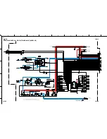
Page 48: ...MP OP AMP DEMULTIPLEXER to P 3 A 4 to P 3 A 4 From P 2 G 4 From P 1 G 4 From P 3 G 2 From P 3 G 2 to P 5 C 1 to P 5 G 4 to P 5 C 3 to P 3 G 5 From P 5 G 4 From P 5 G 5 From P 5 G 5 From P 5 G 4 From P...

Page 49: ...OP AMP to P 4 G 1 to P 3 G 5 to P 2 G 1 to P 1 G 5 to P 4 D 2 to P 3 G 4 to P 3 G 4 to P 4 G 1 to P 4 G 1 to P 3 G 5 to P 2 G 1 to P 1 G 5 to P 4 G 1 to P 4 G 2 From P 4 D 2 From P 4 D 3 to P 4 G 2 3...

Page 50: ...H G F E D C B A 1 2 3 4 5 EMX66M EMX66M EMX66M EMX66M P 6 DSP OP AMP INVERTER EEPROM 1K MIC DSP DRAM 4M ADC 38CC1 8822165 2 1 to MIX66 CN901 EMX66M OVERALL CIRCUIT DIAGRAM 6 7 DSP...

Page 51: ...1 OUTPUT 2 COMMON 3 INPUT PWR1 4 IC103 RBV 1306 V2261600 DIODE STACK 13 0A 600V PWR1 4 D153 1SS133 1SS176 HSS104 VD631600 DIODE 1 2 1 ANODE 2 CATHODE PWR1 4 D101 108 112 113 122 125 128 131 132 139 MT...

Page 52: ...ts The mark in the remarks column indicates that these parts are interchangeable The second letter of the shaded part number is O not zero The second letter of the shaded part number is I not one Note...

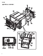
Page 53: ...2 EMX66M OVERALL ASSEMBLY UPC Label 80 70 10 41 42 43 60 40 50 100 B40 B120 B110 B10 B40 B40 B30 B50 B60 B20 B80 B90 B70 B130 90 44 44 110...

Page 54: ...d Head Screw Label Date Code BODY ASSEMBLY Body Assembly Body Assembly Sub Front Frame Sub Handle Assembly Bind Head Tapping Screw P Bind Head Screw Side Plate Bind Head Screw Side Plate Bind Head Scr...

Page 55: ...4 EMX66M FRONT PANEL ASSEMBLY 150 160 130 170 180 120 240 30 100 110 200 190 41 40 10 20 230 220 210 70 60 80 50 60 70 80 90...

Page 56: ...r Switch Knob Circuit Board Bind Head Tapping Screw B Shield Case Bind Head Tapping Screw B Connector Assembly Connector Assembly Connector Assembly Bind Head Screw Button Shield Plate Bind Head Tappi...

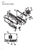
Page 57: ...6 EMX66M REAR PANEL ASSEMBLY 130 170 240 160 140 220 230 30b 30c 30d 40 30a 50 20 80 60 90 10 70 110 100 120 180 150 240 150...

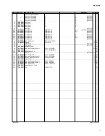
Page 58: ...t Board Circuit Board Circuit Board Circuit Board Bind Head Screw Support TR Holder A TR Holder B Insulation Sheet Bind Head Tapping Screw B Fan Angle Bracket Fan Support Bind Head Screw Bind Head Tap...

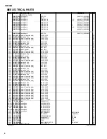
Page 59: ...lectrolytic Cap Ceramic Capacitor chip Ceramic Capacitor chip Electrolytic Cap Ceramic Capacitor chip Ceramic Capacitor chip Electrolytic Cap Ceramic Capacitor chip Electrolytic Cap Electrolytic Cap E...

Page 60: ...chip Carbon Resistor chip Carbon Resistor chip Carbon Resistor chip Flame Proof C Resistor Flame Proof C Resistor Carbon Resistor chip Carbon Resistor chip Carbon Resistor chip Carbon Resistor chip C...

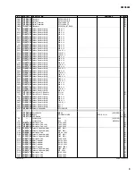
Page 61: ...p Mylar Capacitor Mylar Capacitor Mylar Capacitor Mylar Capacitor Ceramic Capacitor chip Ceramic Capacitor chip Electrolytic Cap Electrolytic Cap Electrolytic Cap Ceramic Capacitor chip Ceramic Capaci...

Page 62: ...apacitor chip Ceramic Capacitor chip Ceramic Capacitor chip Electrolytic Cap Electrolytic Cap Ceramic Capacitor chip Ceramic Capacitor chip Ceramic Capacitor chip Ceramic Capacitor chip Ceramic Capaci...

Page 63: ...lytic Cap Electrolytic Cap Ceramic Capacitor chip Ceramic Capacitor chip Ceramic Capacitor chip Mylar Capacitor Mylar Capacitor Mylar Capacitor Mylar Capacitor Mylar Capacitor Mylar Capacitor Mylar Ca...

Page 64: ...nector Phone Jack Phone Jack XLM Connector Phone Jack Phone Jack Phone Jack Pin Jack Phone Jack Phone Jack Phone Jack Phone Jack LED LED LED LED LED LED LED LED LED LED 0 0100 50V K 100 00 35 0V 0 100...

Page 65: ...or Carbon Resistor chip Metal Film Resistor Metal Film Resistor Flame Proof C Resistor Carbon Resistor chip Carbon Resistor chip Carbon Resistor chip Carbon Resistor chip Carbon Resistor chip Carbon R...

Page 66: ...Resistor chip Carbon Resistor chip Carbon Resistor chip Carbon Resistor chip Carbon Resistor chip Carbon Resistor chip Carbon Resistor chip Carbon Resistor chip Carbon Resistor chip Carbon Resistor ch...

Page 67: ...on Resistor chip Carbon Resistor chip Carbon Resistor chip Carbon Resistor chip Carbon Resistor chip Carbon Resistor chip Carbon Resistor chip Carbon Resistor chip Carbon Resistor chip Carbon Resistor...

Page 68: ...stor chip Carbon Resistor chip Carbon Resistor chip Carbon Resistor chip Carbon Resistor chip Carbon Resistor chip Carbon Resistor chip Carbon Resistor chip Carbon Resistor chip Carbon Resistor chip C...

Page 69: ...chip Carbon Resistor chip Carbon Resistor chip Carbon Resistor chip Carbon Resistor chip Carbon Resistor chip Carbon Resistor chip Carbon Resistor chip Carbon Resistor chip Carbon Resistor chip Carbon...

Page 70: ...istor Rotary Variable Resistor Rotary Variable Resistor Rotary Variable Resistor Rotary Variable Resistor Rotary Variable Resistor Rotary Variable Resistor Rotary Variable Resistor Rotary Variable Res...

Page 71: ...00 V8264600 VV044600 VV044600 VV044600 VV044600 VV044600 VV044600 VV044600 V8264600 V8264600 AAX32870 AAX32880 AAX32890 AAX32900 AAX32910 AAX32920 AAX32930 VV319600 UR896220 UR896220 UR838100 UR838100...

Page 72: ...53900 VZ353500 UR877100 UA953220 UR877100 UR877100 UR896220 UR896220 V5482000 V5482000 V3280500 V3280500 V5482000 V5482000 VY897000 VY897000 UR896470 VV082200 VV082200 V3148500 UR896220 UR896220 V3148...

Page 73: ...102300 V4668300 V4668300 GE300670 GE300670 VR150900 VR150900 VL965100 VL964800 IC1815M0 IA097030 IC1815M0 IA097030 IC224030 IC224030 IA097030 IA097030 IC1815M0 IA097030 IC1815M0 VU418400 VU418600 VU41...

Page 74: ...36 R137 R138 R139 142 R143 R144 VU418400 VD678500 VS883400 V2797700 VU418600 VU418400 VR732800 VR732800 V5611000 V5611000 V5611000 V5611000 VR732800 VR732800 V5611000 V5611000 V5611000 V5611000 VR7328...

Page 75: ...R174 R175 R176 R177 R178 R179 R180 R181 R182 R183 R184 R185 R186 R187 R188 R189 R190 R191 R192 R193 R194 R195 R196 R197 R198 R199 R200 R201 R202 R203 R204 R205 R206 R207 R208 R209 R210 R211 R212 R213...

Page 76: ...nsformer Power Transformer Power Transformer Fan R217 R218 R219 R220 R221 R222 225 R226 231 R232 R233 RY101 RY102 SW101 W101 W101a W102 W103 VZ370200 VV313600 VZ370200 VV313600 VZ370200 VV276700 VV276...

Page 77: ...26 EMX66M RK 88 RACK MOUNT KIT 10 20 REF NO PART NO DESCRIPTION REMARKS QTY RANK VB132700 RACK MOUNT KIT Bind Head Screw Rack Angle 4 0X12 MFZN2BL RK 88 V840830 01 10 20 6 2 RANK Japan only New Parts...

Reviews: