background image

adjustment SUB-BRIGHT to let picture on the screen microbright. 

4.5

 receive white balance adjustment signal 

enter PAGE3 of factory menu, press PP to select T1 picture mode, let the value of GD unchange, adjust 
RD and B.D to let the white part of the picture appear “white”. 

4.6

 Use white balancer to rectify the white balance under following conditions   

colour temperature:8MPCD   
  x =0.270± 0.008 Y=0.283±0.008    dark space : 4.5nit, bright space: 60nit 

Note:

1. Check the white balance of bright field and dark field by receiving monochrome signal or 

adjusting the degree of saturation to minimum under maintenance condition, adjust RGB BIAS in dark 
field and RGB DRIVE in bright area, adjust bright/dark balance repeatedly until the bright and dark 
field have no colour drift. 

2. While the colour saturation changed from maximum to minimum, if the dark balance appears 

changeable, adjust RY.DC.LVL and BY.DC.LVL (page3) to let it coincide with white balance. 

3. If the dark balance appears changeable while connected with DVD, adjust YUV.BY.DC and 
YUV.RY.DC (PAGE4) to let it conincide with white balance. 

4.7 High voltage and filament voltage check 

Connect a high-voltage meter between anode cap of picture tube and the ground, measure the filament 
voltage using rms voltmeter, set the picture mode to “standard”, the high-voltage: 24.5KV±1KV of 21”, 
22.5KV±1KV of 14”,filament voltage: 6.3±0.1Vrms. 

4.8 x -ray protection check 

Receive local TV signal, set the picture mode to “standard”, shorten the circuit and measure the 

value of TP1-TP2, restart the TV 30 seconds after turn off the power source and it should return to 
normal. 

4.9  

AV function check 

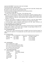
according to the owner’s manual require, connect to the AV equipment and the AV interface: 

VIDEO IN: 

1 Vp-p 75OHM 

AUDIO IN: 

(-8±3)dBm>47 kOHM 

S interface Y IN: 

1 Vp-p 75OHM 

C IN: 

0.3 Vp-p 75OHM 

DVD Y IN: 

1 Vp-p 75OHM 

Cr IN: 

0.7 Vp-p 75OHM 


Cb IN: 

0.7 Vp-p 75OHM 


4.10  AV parts check


incept to standard the TV signal: 
a

 AV and crossfire and allophone and shake ; 

b

 The user control function ana picture model 

c

 The remote control function check; 

d

 Color pure and converge check. 

4.11    leave factory state setup


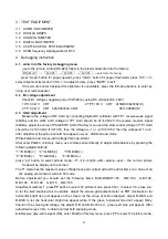
Picture model (PP) 

STENDARD 

language 

All the country language 

Color system 

AUTO 

C.CAPTION C1 
CCD ON MUTE 

OFF 

RECEPTION AIR 
AFT ON 

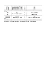
Summary of Contents for TK2055D

Page 1: ...COLOR TELEVISION TS2049 TK2055D...

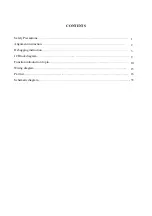
Page 2: ...CONTENTS Safety Precautions Alignment instruction Debugging instruction IC Block diagram Function introduction to pin Wiring diagram Part list Schematic diagram 1 2 3 9 10 15 16 35...

Page 3: ...elow 1 2 SAFETY PRECAUTION WARNING Service should not be attempted by anyone unfamiliar with the necessary precaution on this receiver The following are the necessary precautions to be observed before...

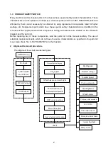
Page 4: ...placing any of these components read the parts list in this manual carefully The use of substitute replacement parts which do not have the same characteristics as specified in the parts list may creat...

Page 5: ...or 2 if V2 3 5V then the voltage is 1 or 2 after adjustment the picture should not appear no sync distortion and moire White balance and screen grid voltage VG2 adjustment After enter PAGE3 of factory...

Page 6: ...BY DC and YUV RY DC PAGE4 to let it conincide with white balance 4 7 High voltage and filament voltage check Connect a high voltage meter between anode cap of picture tube and the ground measure the...

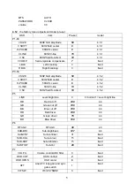
Page 7: ...5 2 H PHASE 50HZ H center 6 4 5 2 V LINE 50HZ V line 13 4 5 2 V SC 50HZ field S correct 10 4 5 2 P5 LINE Level bright line 0 0 normal 1 Level bright line RB Red cut off 100 4 4 GB Green cut off 100 4...

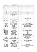
Page 8: ...C PRE ADJ Pre shoot 3 fixed 0 narrow 3 width OVER ADJ overshoot 3 Fixed a 0 narrow 3 width C VCO ADJ Color VCO frequency adjustment 4 fixed 0 4 7 120KHZ 0 90KHZ P10 BRT ABL DEF Brightness ABL 0 fixed...

Page 9: ...tic level 5 fixed 0 30dB 3 40dB VCO FREQ VCO frequency 32 fixed P14 Y GAIN 0 fixed Y TH 0 fixed B OFFSET 0 fixed B WIDTH 0 fixed C OFFSET 0 fixed C WIDTH 0 fixed CAN V CHIP V CHIP 0 1 1 CAN V CHIP OPT...

Page 10: ...xed VOL 75 75 volume control speciality 82 fixed 72700 ALC ALC 1 fixed 1 ALC ON VOL Baseband model input level adjustment 0 The unit no use SAP LEVEL SAP level 1 fixed SIF M BB M SIF and baseband mode...

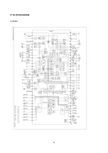
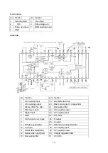
Page 11: ...9 IC BLOCK DIAGRAM LA76931...

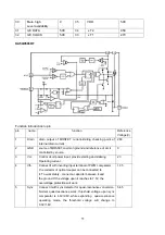
Page 12: ...panded video input and Y input 2 50 12 R ouput 2 65 53 Colour APC filter 3 40 13 G ouput 2 65 52 Selection video output and FSC output 2 40 14 B ouput 2 67 51 Cr input 2 50 15 AKB undo 2 31 50 4 43 MH...

Page 13: ...cicuit power input provide starting and stabling Operating current 23 4 Vfb Connect it with inverting input terminal of PWM comparator the collector of optical coupler can be connected to it To work s...

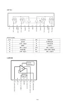
Page 14: ...12 AN7522 Pins function pin function pin function 1 power 7 GND input 2 CH1 output 8 CH2 input 3 GND 9 volume 4 CH1 output 10 CH1 output 5 Stand by 11 GND CH2 output 6 CH1 input 12 CH1 output LA78040...

Page 15: ...l input 23 AC coupling input 6 GND 24 ALC filter 7 SAP carrier level check 25 R output 8 26 L output 9 SIF decoupling filter 27 Reference voltage DC3 8V 10 mute 5V 28 AC coupling input 11 Serial data...

Page 16: ...V STEREO 3 0V STEREO SAP 3 8V 15 SAP detection sensitivity 33 Sub carrier input 3 579545MHZ 200Mv 16 dbx RMS detection 34 Filter adjustment check 17 Dbx broad band detection 35 Pilot dispel reference...

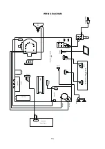
Page 17: ...XS501 XS202 XS203 XS701 TUNER XS601 XS602 XS301 XS604 XS201 XS302 N201 XS502 CRT DEGASSINGP COIL M108 FOCUS SCREEN MAIN BOARDP667 TSC30 01 POWER SWITCH KEY BOARDP667 TS2130 05 XS901 XS902 SPEAKER XS60...

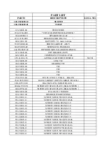
Page 18: ...RV105 12X0 15 370mm BLACK 780 10973U020 BACK CABINET HIPS V0 MOLD BLACK 808 10557 020 BLACK PLATE MOLD BLACK 808 6A799 07A INTERFACE SPACE PLATE SILK SCREEN 808 6F758 02 INTERFACE SPACE PLATE SILK SC...

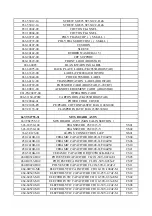
Page 19: ...RD ASS Y 667 TS2755 31 MTS BOARD ASS Y MANUAL INSERTION 343 18150 104 TRANSISTOR 2SC1815 Y VS01 343 18150 104 TRANSISTOR 2SC1815 Y VS02 364 3E123 00 40 PINS CONNECTORS L40P XS01 459 2410R 00 CERAMIC C...

Page 20: ...0 68uH K LS01 998 JUMPER WIRE WS01 667 Q2735 31 MTS BOARD ASS Y SMD 353 58320 50 SMD ICAN5832SA D NS01 782 Q2735 310B STEREO PCB 667 TS2129 05 KEY BOARD ASS Y 360 10070 00 TACT SWITCH EVQPC105K SW901...

Page 21: ...80 TO 126 V502 343 21400 00 TRANSISTOR TT2140 V302 343 26880 20 TRANSISTOR 2SC2688L V401 343 26880 20 TRANSISTOR 2SC2688L V402 343 26880 20 TRANSISTOR 2SC2688L V403 352 04310 00 IC LM431A M N504 352 0...

Page 22: ...F J C304 462 83433 H0 POLYESTER CAPACITOR CBB21 200V 0 33uF J C339 462 88239 H0 POLYESTER CAPACITOR CBB81 1600V 3900pF J C310 462 88256 H0 POLYESTER CAPACITOR ECWH12H562JR C311 462 B0410 H0 POLYESTER...

Page 23: ...67 8E227 H0A SOLID RESISTOR 1 2W 2 7K J R417 467 8E227 H0A SOLID RESISTOR 1 2W 2 7K J R418 467 8E422 H0 SOLID RESISTOR 1 2W 220K JL R504 467 8E522 H0A SOLID RESISTOR 1 2W 2 2M J R501 467 8E582 H0A SOL...

Page 24: ...REW P T3X8S R N301 851 13008 56 SCREW P T3X8S R N501 851 13008 56 SCREW P T3X8S R N701 851 13008 56 SCREW P T3X8S R N701 851 23012 11 SCREW SJ2824 ST3X12C DZn 851 23012 11 SCREW SJ2824 ST3X12C DZn 851...

Page 25: ...JUMPER WIRE J013 998 JUMPER WIRE J014 998 JUMPER WIRE J015 998 JUMPER WIRE J016 998 JUMPER WIRE J017 998 JUMPER WIRE J018 998 JUMPER WIRE J019 998 JUMPER WIRE J020 998 JUMPER WIRE J021 998 JUMPER WIRE...

Page 26: ...UMPER WIRE J061 998 JUMPER WIRE J062 998 JUMPER WIRE J063 998 JUMPER WIRE J064 998 JUMPER WIRE J065 998 JUMPER WIRE J066 998 JUMPER WIRE J067 998 JUMPER WIRE J068 998 JUMPER WIRE J069 998 JUMPER WIRE...

Page 27: ...003 DIODE 1N4148 VD403 340 00001 003 DIODE 1N4148 VD502 340 00001 003 DIODE 1N4148 VD506 340 00001 003 DIODE 1N4148 VD510 340 00001 003 DIODE 1N4148 VD512 340 00001 003 DIODE 1N4148 VD601 340 00001 0...

Page 28: ...H1H101JYR C712 459 2110H 102 CERAMIC CAPACITOR CC45 CH1H101JYR C713 459 2110H 102 CERAMIC CAPACITOR CC45 CH1H101JYR C714 459 2120H 902 CERAMIC CAPACITOR RBU06SL201J H46CA C252 459 2127H 902 CERAMIC CA...

Page 29: ...245 462 B0410 H02 POLYESTER CAPACITOR CL21X 50V 0 1uF J C520 462 B0447 H02 POLYESTER CAPACITOR CL21X 50V 0 47uF J C214 462 B0510 H02 POLYESTER CAPACITOR CL21X 50V 1uF J C217 464 30447 M02 ELECTROLYTIC...

Page 30: ...0 16V 10uF M C710 464 6D622 M02 ELECTROLYTIC CAPACITOR CD110 16V 22uF M C211 464 6D647 M02 ELECTROLYTIC CAPACITOR CD110 16V 47uF M C255 464 6D710 M02 ELECTROLYTIC CAPACITOR CD110 16V 100uF M C212 464...

Page 31: ...390 J R409 467 1C147 H03 CARBON RESISTOR 1 6W 470 J R519 467 1C156 H03 CARBON RESISTOR 1 6W 560 J R231 467 1C156 H03 CARBON RESISTOR 1 6W 560 J R234 467 1C156 H03 CARBON RESISTOR 1 6W 560 J R240 467 1...

Page 32: ...1 6W 10K J R204 467 1C310 H03 CARBON RESISTOR 1 6W 10K J R206 467 1C310 H03 CARBON RESISTOR 1 6W 10K J R226 467 1C310 H03 CARBON RESISTOR 1 6W 10K J R236 467 1C310 H03 CARBON RESISTOR 1 6W 10K J R325...

Page 33: ...J R618 467 1C415 H03 CARBON RESISTOR 1 6W 150K J R225 467 1C415 H03 CARBON RESISTOR 1 6W 150K J R343 467 1C415 H03 CARBON RESISTOR 1 6W 150K J R344 467 1C439 H03 CARBON RESISTOR 1 6W 390K J R207 467...

Page 34: ...COPPER M127 895 6020025 50 RIVET GB876 86 2X2 5 COPPER M128 895 6020025 50 RIVET GB876 86 2X2 5 COPPER M129 895 6020025 50 RIVET GB876 86 2X2 5 COPPER M132 895 6020025 50 RIVET GB876 86 2X2 5 COPPER M...

Page 35: ...K 5 LA02 655 6E301 12 6 PINS LEAD WITH HOUSING XA02 782 TS2049 2900 SIDE AV PCB 851 23010 11 SCREW SJ2824 ST3X10C D Zn 868 20037 00 FIBRE WASHER 8X 3 2X0 5 870 20884 00 SIDE AV BRACKET 667 TS20491 05...

Page 36: ...I ST O VCC9V MODE O LA72700 NS01 S R DET NS01 LA72700 CS05 1uF CS06 0 1uF CS07 0 1uF RS02 100 RS03 100 CS08 0 1uF CS09 22uF CS10 4 7uF CS11 4 7uF CS12 3 3uF CS13 4 7uF CS14 4 7uF CS15 1uF CS 4n7 CS16...

Page 37: ...ON C612 16V 10u C613 16V 10u R614 100K G V1 R1 V2 R2 G L2 R517 5K6 R515 5K6 R243 10K R527 100K C527 10n KEY KEY S C V OUT V OUT REM REM 9V Y DVD G 1 2 3 4 5 6 7 8 9 10 11 12 13 14 15 16 N601 TC4053 R6...

Reviews: