background image

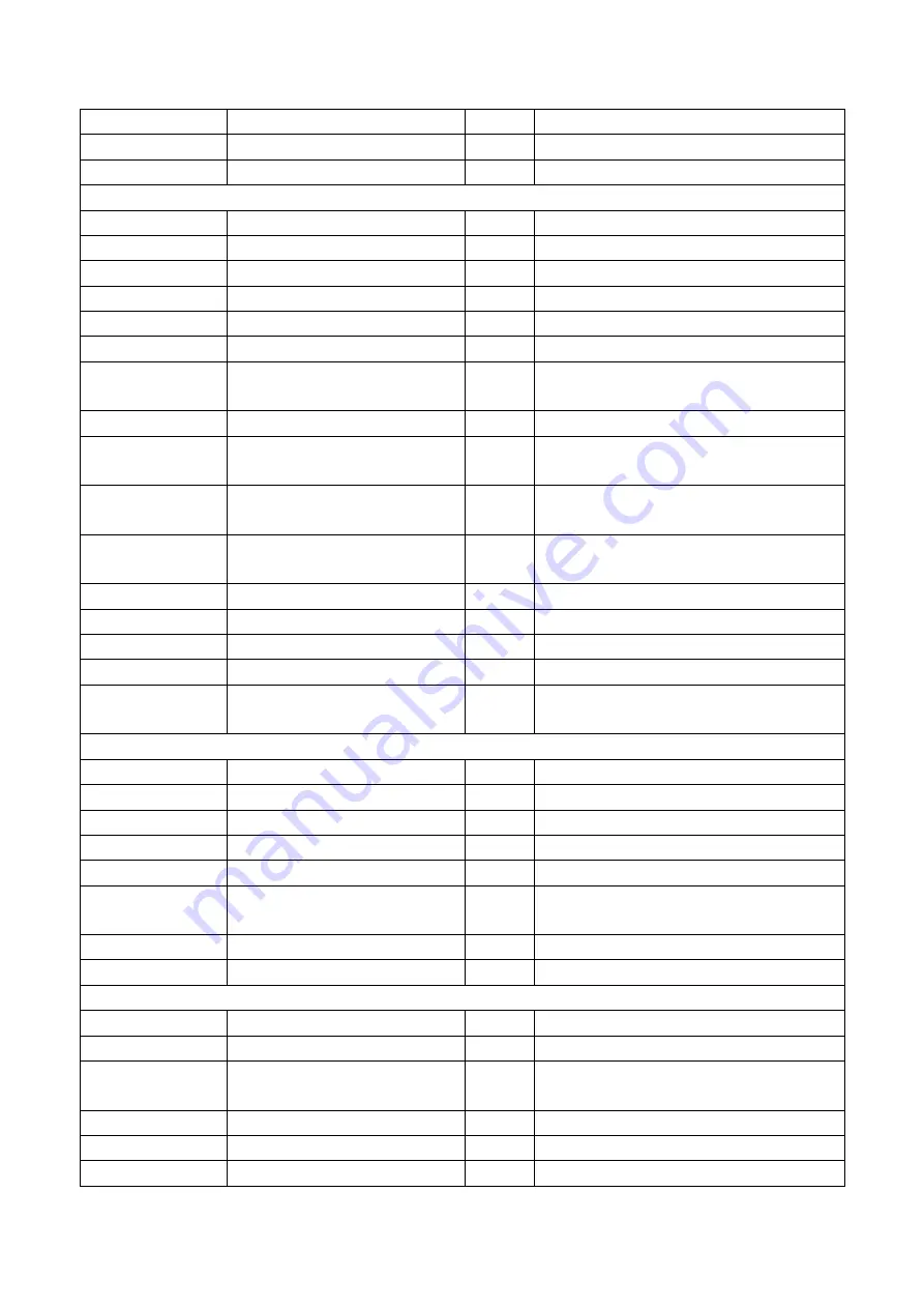
SIF SW 

Sound IF0=4.5MHZ 

fixed 

VIDEO LEVEL 

VIDEO LEVEL 


 3 

fixed 


P8 

GY ANGLE 

G-Y demodulation angle 

fixed 

V.R TM 

Filed scan strting time 

fixed 

R/B ANG 

R-Y/B-Y demodulation angle 

Fixed 

R/B BAL 

R-Y/B-Ydemodulation balance

fixed 

C TRAP 

Color trap filter 

fixed 

H FREQ 

H-frequency 

16 

fixed 

C.BPF TEST 

Color band filter center 

frequency 

0 fixed 

P9  


OVER.MOD.SW 

Selection over-modulation 

function 

0 Fixed,0=nothing 

1=have 

   
OVER.MOD.LVL 

Adjustment over-modulation 

working point 

0 fixed 

BLK.STR 

Dark level expand starting 

control point 

Fixed,0=40IRE 2=60IRE 3-OFF 

BLK.GAIN 

Dark level expand gain 

Fixed,0=MIN 2=MAX 

Y.APF 

Selection color trap filter 

0=trap filter,1= direct pass(YcbCr&Y/C)

PRE.ADJ Pre-shoot 

fixed, 0=narrow 3=width 

OVER ADJ 

overshoot 

Fixed,a 0=narrow 3=width 

C.VCO.ADJ 

Color VCO frequency 

adjustment 

fixed,0

4

7=-120KHZ-0-90KHZ 

P10 

BRT.ABL.DEF 

Brightness ABL 

fixed,0=ABL ON 1=ABL OFF 

MID.STP.DEF 

ABL start control point 

fixed 

BRT.ABL.THR ABL 

threshold  7 

fixed 

WPL.OPE 

White peak limit 

fixed 

V BLK.SW 

Field blanking switch 

fixed ,0=nomarl;1=width model   

FBP BLK SW 

Horizontal blanking switch 

fixed,0=inside produce;1=FBP and 

inside logic “and” 

DC REST 

DC recover rate 

fixed,0=100% 1=107% 

CD.MODE 

Field frequency division model

fixed,0=auto 

P11 

CORE GAIN 

Noise reduction 

fixed,0=OFF 1=MIN 3=MAX 

γ

.GAMA 

r-correct 0 

fixed,0=OFF 

RGB TEMP.SW 

RGB DC output 

temperature speciality 

1 fixed 

A.MONI SW 

Selection pin5 output   

fixed

1=SAO 

SVO OR FSC 

Selection pin5 output 

fixed,0=VIDEO 1=FSC(color sub-carrier wave)

CROSS B/W 

Selection test signal 

fixed,0=TV 

Summary of Contents for NXT1333

Page 1: ...COLOR TELEVISION TS1333 NXT1333...

Page 2: ...CONTENTS Safety Precautions Alignment instruction Debugging instruction IC Block diagram Function introduction to pin Wiring diagram Exploded view Part list Schematic diagram 1 2 3 9 10 15 16 18 33...

Page 3: ...elow 1 2 SAFETY PRECAUTION WARNING Service should not be attempted by anyone unfamiliar with the necessary precaution on this receiver The following are the necessary precautions to be observed before...

Page 4: ...placing any of these components read the parts list in this manual carefully The use of substitute replacement parts which do not have the same characteristics as specified in the parts list may creat...

Page 5: ...or 2 if V2 3 5V then the voltage is 1 or 2 after adjustment the picture should not appear no sync distortion and moire White balance and screen grid voltage VG2 adjustment After enter PAGE3 of factory...

Page 6: ...BY DC and YUV RY DC PAGE4 to let it conincide with white balance 4 7 High voltage and filament voltage check Connect a high voltage meter between anode cap of picture tube and the ground measure the...

Page 7: ...5 2 H PHASE 50HZ H center 6 4 5 2 V LINE 50HZ V line 13 4 5 2 V SC 50HZ field S correct 10 4 5 2 P5 LINE Level bright line 0 0 normal 1 Level bright line RB Red cut off 100 4 4 GB Green cut off 100 4...

Page 8: ...C PRE ADJ Pre shoot 3 fixed 0 narrow 3 width OVER ADJ overshoot 3 Fixed a 0 narrow 3 width C VCO ADJ Color VCO frequency adjustment 4 fixed 0 4 7 120KHZ 0 90KHZ P10 BRT ABL DEF Brightness ABL 0 fixed...

Page 9: ...tic level 5 fixed 0 30dB 3 40dB VCO FREQ VCO frequency 32 fixed P14 Y GAIN 0 fixed Y TH 0 fixed B OFFSET 0 fixed B WIDTH 0 fixed C OFFSET 0 fixed C WIDTH 0 fixed CAN V CHIP V CHIP 0 1 1 CAN V CHIP OPT...

Page 10: ...xed VOL 75 75 volume control speciality 82 fixed 72700 ALC ALC 1 fixed 1 ALC ON VOL Baseband model input level adjustment 0 The unit no use SAP LEVEL SAP level 1 fixed SIF M BB M SIF and baseband mode...

Page 11: ...9 IC BLOCK DIAGRAM LA76931...

Page 12: ...panded video input and Y input 2 50 12 R ouput 2 65 53 Colour APC filter 3 40 13 G ouput 2 65 52 Selection video output and FSC output 2 40 14 B ouput 2 67 51 Cr input 2 50 15 AKB undo 2 31 50 4 43 MH...

Page 13: ...cicuit power input provide starting and stabling Operating current 23 4 Vfb Connect it with inverting input terminal of PWM comparator the collector of optical coupler can be connected to it To work s...

Page 14: ...12 AN7522 Pins function pin function pin function 1 power 7 GND input 2 CH1 output 8 CH2 input 3 GND 9 volume 4 CH1 output 10 CH1 output 5 Stand by 11 GND CH2 output 6 CH1 input 12 CH1 output LA78040...

Page 15: ...l input 23 AC coupling input 6 GND 24 ALC filter 7 SAP carrier level check 25 R output 8 26 L output 9 SIF decoupling filter 27 Reference voltage DC3 8V 10 mute 5V 28 AC coupling input 11 Serial data...

Page 16: ...V STEREO 3 0V STEREO SAP 3 8V 15 SAP detection sensitivity 33 Sub carrier input 3 579545MHZ 200Mv 16 dbx RMS detection 34 Filter adjustment check 17 Dbx broad band detection 35 Pilot dispel reference...

Page 17: ...XS501 XS202 XS203 XS701 TUNER XS601 XS602 XS301 XS604 XS201 XS302 N201 XS502 CRT DEGASSINGP COIL M108 FOCUS SCREEN MAIN BOARDP667 TSC30 01 POWER SWITCH KEY BOARDP667 TS2130 05 XS901 XS902 SPEAKER XS60...

Page 18: ...1 2 3 4 5 6 7 8 9 11 10 12 13 14 15 16 17 18 19 20 21 22 23 24 25 EXPLODED VIEW...

Page 19: ...CABIINET ASSY 611 B33R6 0H1 11 STANDBY BUTTON 877 60536 H0 12 SPEAKER 384 40916 J0 13 FRONT NAMEPLATE 880 10785 A1 14 SIDE AV BOARD ASSY 667 TS1433 29A 15 BUTTON BOARD ASSY 667 TS1333 05A 16 MAIN BOA...

Page 20: ...CK CRT G 780 10887 20 BACK CABINET MOLD BLACK 785 30002 09A RUBBER BAND 808 6A758 02 AV BAFFLE SILK SCREEN 808 70239 00 EVA GLUE 150X50X1 838 10164 00 BRAIDED WIARE SPRING 851 23012 11 SCREW SJ2824 ST...

Page 21: ...MAIN PCB ASS Y MANUAL INSERTION 998 JUMPER WIRE C203 998 JUMPER WIRE N601 998 JUMPER WIRE R314 998 JUMPER WIRE XS601 998 JUMPER WIRE XS603 998 JUMPER WIRE XS606 998 JUMPER WIRE XS701 329 33204 00 CRYS...

Page 22: ...ACITOR CL11 100V 0 1uF K C326 462 00410 K0 POLYESTER CAPACITOR CL11 100V 0 1uF K C328 462 2B410 M0U POLYESTER CAPACITOR MKP 300VAC 0 1UF M C502 462 2B422 M0U POLYESTER CAPACITOR 250VAC 0 22uF M C501 4...

Page 23: ...7 8E227 H0A SOLID RESISTOR 1 2W 2 7K J R417 467 8E227 H0A SOLID RESISTOR 1 2W 2 7K J R418 467 8E422 H0 SOLID RESISTOR 1 2W 220K JL R504 467 8E522 H0A SOLID RESISTOR 1 2W 2 2M J R501 467 8E582 H0A SOLI...

Page 24: ...81 SCREW P M3X8 D Zn N503 852 13008 81 SCREW P M3X8 D Zn V302 852 13008 81 SCREW P M3X8 D Zn V502 881 60074 00 HIGH VOLTAGE WARNING LABEL 893 10300 11 NUT GB6170 86 M3 D Zn N503 893 10300 11 NUT GB617...

Page 25: ...UMPER WIRE J044 998 JUMPER WIRE J045 998 JUMPER WIRE J047 998 JUMPER WIRE J048 998 JUMPER WIRE J049 998 JUMPER WIRE J050 998 JUMPER WIRE J051 998 JUMPER WIRE J052 998 JUMPER WIRE J053 998 JUMPER WIRE...

Page 26: ...IRE J101 998 JUMPER WIRE J102 998 JUMPER WIRE J103 998 JUMPER WIRE J104 998 JUMPER WIRE J106 998 JUMPER WIRE J401 998 JUMPER WIRE R316 998 JUMPER WIRE R420 998 JUMPER WIRE R421 998 JUMPER WIRE R422 99...

Page 27: ...CC45 CH1H101JYR C714 459 2120H 902 CERAMIC CAPACITOR RBU06SL201J H46CA C252 459 2127H 902 CERAMIC CAPACITOR CC45 SL1H271JYR C404 459 2127H 902 CERAMIC CAPACITOR CC45 SL1H271JYR C405 459 2127H 902 CER...

Page 28: ...F M C239 464 60510 M02 ELECTROLYTIC CAPACITOR CD110 50V 1uF M C242 464 60510 M02 ELECTROLYTIC CAPACITOR CD110 50V 1uF M C243 464 60510 M02 ELECTROLYTIC CAPACITOR CD110 50V 1uF M C247 464 60510 M02 ELE...

Page 29: ...OR 1 6W 75 J R601 467 1C075 H03 CARBON RESISTOR 1 6W 75 J R602 467 1C075 H03 CARBON RESISTOR 1 6W 75 J R603 467 1C075 H03 CARBON RESISTOR 1 6W 75 J R604 467 1C075 H03 CARBON RESISTOR 1 6W 75 J R609 46...

Page 30: ...7 1C239 H03 CARBON RESISTOR 1 6W 3 9K J R522 467 1C243 H03 CARBON RESISTOR 1 6W 4 3K J R611 467 1C247 H03 CARBON RESISTOR 1 6W 4 7K J R210 467 1C247 H03 CARBON RESISTOR 1 6W 4 7K J R313 467 1C247 H03...

Page 31: ...238 467 1C368 H03 CARBON RESISTOR 1 6W 68K J R242 467 1C410 H03 CARBON RESISTOR 1 6W 100K J R101 467 1C410 H03 CARBON RESISTOR 1 6W 100K J R527 467 1C410 H03 CARBON RESISTOR 1 6W 100K J R614 467 1C410...

Page 32: ...RIVET GB876 86 2 5X3 COPPER M201 895 6025030 50 RIVET GB876 86 2 5X3 COPPER M202 895 6025030 50 RIVET GB876 86 2 5X3 COPPER M203 895 6025030 50 RIVET GB876 86 2 5X3 COPPER M204 895 6025030 50 RIVET GB...

Page 33: ...TS1433 29A SIDE AV BOARD ASS Y 364 11205 00 EARPHONE JACK 3F27K XV05 364 36101 00 6 PINS CONNECTORS TJC3 06A XV04 364 93202 00 AV JACK AV306 2 XA01 464 6D647 M0 ELECTROLYTIC CAPACITOR CD110 16V 47uF M...

Page 34: ...I ST O VCC9V MODE O LA72700 NS01 S R DET NS01 LA72700 CS05 1uF CS06 0 1uF CS07 0 1uF RS02 100 RS03 100 CS08 0 1uF CS09 22uF CS10 4 7uF CS11 4 7uF CS12 3 3uF CS13 4 7uF CS14 4 7uF CS15 1uF CS 4n7 CS16...

Page 35: ...ON C612 16V 10u C613 16V 10u R614 100K G V1 R1 V2 R2 G L2 R517 5K6 R515 5K6 R243 10K R527 100K C527 10n KEY KEY S C V OUT V OUT REM REM 9V Y DVD G 1 2 3 4 5 6 7 8 9 10 11 12 13 14 15 16 N601 TC4053 R6...

Reviews: