3
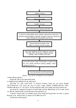
Figure 1. Flow process of adjustment and calibration
3.Flash writing programs
Flash write memory N4, N20, N303, N302
4.Adjustment and calibration for the main board
a)Connect the main board X501 to infrared receiving board (as per wiring diagram
203-L15H30-01JL) and insert the plug of power supply adapter (FSP048-1AD101C for15”,
FSP060-1AD103 for 17”, 20”) into X1. Now the indication lamp of the infrared receiving board is red.
b)Connect PC, upgrade the program of FLASH N20, push the POWER key on the remote control
set. Now the indication lamp of the infrared receiving board is out.
c) About 4 minutes later the indication lamp of the infrared receiving board turns blue or yellow.
Measure L102 PIN2 to be5.0 V, measure L107 PIN2 to be 3.3 V.
d) Flash write DDC program.
Input YprPb signal, check if the display is normal under
PC and various functions (analog quantity control,
line/field center etc.)
Check accessories and then packing
Check main board
Check TV board
Combined test for general assembly
Connect to central signal source satellite signal, check if various TV
functions (station skipping, modulate quantity control etc), check if the
output of earphone and speaker are normal
Input AV/S terminal signal, check
different functions of AV/S terminals
Adjust TV board
Input VGA signal and check if display is normal in
the state of PC and various functions (analog
quantity control, line/field center etc.)
Summary of Contents for LC20H3D
Page 1: ...COLOR TELEVISION LC20H3D...
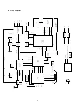
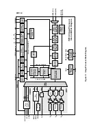
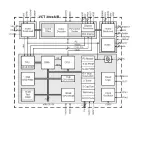
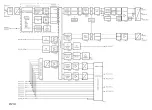
Page 12: ...10 BLOCK DIAGRAM...
Page 14: ......
Page 15: ......
Page 17: ......
Page 18: ......
Page 19: ......
Page 25: ...1 2 3 4 5 6 7 8 9 101112 13 14 15 16 17 18 23 EXPLODED VIEW...
Page 44: ......
Page 45: ......
Page 46: ......
Page 47: ......
Page 48: ......
Page 49: ......
Page 50: ......
Page 51: ......
Page 52: ......
Page 53: ......
Page 54: ......
Page 55: ......


