


ZCU102 Evaluation Board User Guide
92
UG1182 (v1.2) March 20, 2017
Chapter 3:
Board Component Descriptions
PCIe (MIO 31)
The ZCU102 hosts a 4-lane PCIe root port connector similar to those commonly used on
many micro-ATX motherboards. The PS-side GTR transceivers can be set to provide a PCI
Express interface that operates at GEN2 speeds with a width of 1-lane (x1), 2-lanes (x2), or
4-lanes (x4).
The Zynq Ult MPSoC contains an integrated block for PCI Express interface based
on the PCIe base v2.1 specification. The PS-side, PCIe reset signal (PS Bank 501 MIO31 pin
J22) is wired to the PCIe Gen2 x4 root port slot P1. This MIO pin is an output for Root Port
mode operation. The primary purpose of the ZCU102 is for PCIe root port operation.
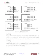
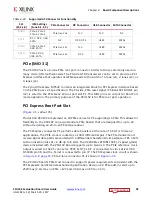
PCI Express Root Port Slot
[
, callout 35]
Production ZCU102s implement an x8 PCIe connector P1 supporting x4 PCIe. This allows for
flexibility so the ZCU102 can accommodate PCIe boards that are designed for up to x8
without requiring an x8-to-x4 PCIe lane reducer.
The PCI Express connector P1 performs data transfers at the rate of 5.0 GT/s for Gen2
applications. The PCIe clock is routed as a 100
Ω
differential pair. The PCIe transmit and
receive signal data paths are routed with a differential characteristic impedance of 85 ±10%
with an insertion loss of <4 dB up to 8 GHz. The XCZU9EG-L2FFVB1156E (-2 speed grade)
device included with the ZCU102 board supports up to Gen3 x4. The PCIe reference clock
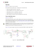
output is wired to the P1 connector. PCIE_SLOT_CLK_P is connected to clock driver U69
Si5341B pin 38, and the _N net is connected to pin 37. The PCI Express clock circuit is shown
in
. PCIe 4-lane connector P1 is shown in
.
The ZCU102 board’s PCIe Host connector supports power requirements consistent with the
PCI Express® Card Electromechanical Specification Revision 2.0 PCIe add-in cards up to
25W max (2.1A max on PCIe +12V and 3.0A max on PCIe +3.3V).
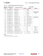
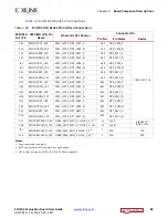
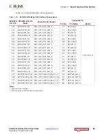
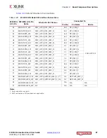
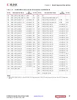
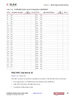
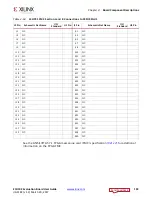
Table 3-43:
Supported GTR Connector Functionality
SEL
(S3,2,1,0)
ICM Settings
(Lane 0,1,2, 3)
PCIe Connector
DP Connector
USB Connector SATA Connector
0000
PCIe.0, PCIe.1,
PCIe.2, PCIe.3
PCIe Gen2 x4
N.C.
N.C.
N.C.
1111
DP.1, DP.0, USB,
SATA
N.C.
DP.0, DP.1
USB0
SATA1
1100
PCIe.0, PCIe.1,
USB, SATA
PCIe Gen2 x2
N.C.
USB0
SATA1
1110
PCIe.0, DP.0,
USB, SATA
PCIe Gen2 x1
DP.0
USB0
SATA1


