


ZCU102 Evaluation Board User Guide
45
UG1182 (v1.2) March 20, 2017
Chapter 3:
Board Component Descriptions
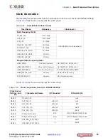
Programmable User Clock
[
, callout 8]
The ZCU102 board has an I2C programmable SI570 low-jitter 3.3V LVDS differential
oscillator (U42) connected to the GC inputs of PL bank 64. This USER_SI570_P and
USER_SI570_N clock signal pair is connected to XCZU9EG MPSoC U1 pins AL8 and AL7
respectively. On power-up the user clock defaults to an output frequency of 300.000 MHz.
User applications can change the output frequency within the range of 10 MHz to 810 MHz
through an I2C interface. Power cycling the ZCU102 board reverts this user clock to the
default frequency of 300.000 MHz.
This oscillator can be reprogrammed from MSP430 system controller U41 (see
for more information).
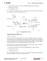
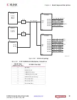
X-Ref Target - Figure 3-8
Figure 3-8:
SI5341B Clock Generator
;


