


ZCU102 Evaluation Board User Guide
70
UG1182 (v1.2) March 20, 2017
Chapter 3:
Board Component Descriptions
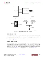
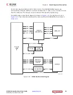
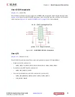
SFP/SFP+ Clock Recovery
[
, callout 11]
The ZCU102 board includes a Silicon Labs Si5328B jitter attenuator U20 (8 kHz - 808 MHz).
The FPGA can output the RX recovered clock to a differential I/O pair on I/O bank 67
(SFP_REC_CLOCK_C_P, pin R10 and SFP_REC_CLOCK_C_N, pin R9) for jitter attenuation.
The jitter attenuated clock (SFP_SI5328_OUT_C_P (U20 pin 28), SFP_SI5328_OUT_C_N (U20
pin 29)) is then routed as a reference clock to GTH Quad 230 inputs MGTREFCLK1P (U1 pin
B10) and MGTREFCLK1N (U1 pin B9).
The primary purpose of this clock is to support synchronous protocols such as CPRI or
OBSAI to perform clock recovery from a user-supplied SFP/SFP+ module and use the jitter
attenuated recovered clock to drive the reference clock inputs of a GTH transceiver. The
system controller configures the SI5328B in free-run mode (see
). Enabling the jitter attenuation feature requires additional user
programming from the FPGA through the I2C bus.The jitter attenuated clock circuit is
shown in
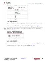
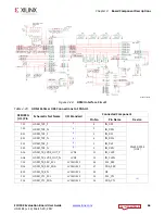
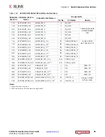
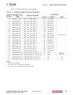
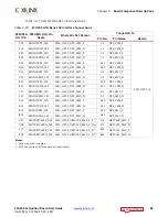
Location Left Lower SFP3
A8
SFP3_TX_P
LL18
LL_TD_P
A7
SFP3_TX_N
LL19
LL_TD_N
A4
SFP3_RX_P
LL13
LL_RD_P
A3
SFP3_RX_N
LL12
LL_RD_N
C13
SFP3_TX_DISABLE
LL3
LL_ TX_DISABLE
Notes:
1. SFPx_TX_DISABLE pins should implement the LVCMOS33 I/O standard.
Table 3-30:
XCZU9EG U1 to P2 SFP+ Module Quad-Connector
(Cont’d)
XCZU9EG
(U1) Pin
Schematic Net Name
SFP+ Pin
SFP+ Pin Name


