background image

Virtex-5 FPGA User Guide

www.xilinx.com

295

UG190 (v5.0) June 19, 2009

Specific Guidelines for I/O Supported Standards

Transmitter Termination 

The Virtex-5 FPGA LVDS transmitter does not require any external termination. 

Table 6-36


lists the allowed attributes corresponding to the Virtex-5 FPGA LVDS current-mode 
drivers. Virtex-5 FPGA LVDS current-mode drivers are a true current source and produce 
the proper (EIA/TIA compliant) LVDS signal.

Receiver Termination

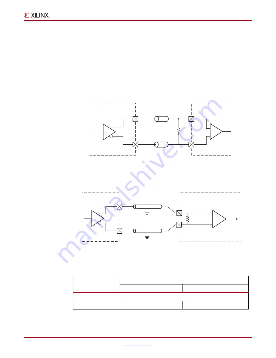
Figure 6-87

 is an example of differential termination for an LVDS receiver on a board with 

50

Ω

 transmission lines.  

Figure 6-88

 is an example of a differential termination for an LVDS receiver on a board with 

50

Ω

 transmission lines. 

Table 6-36

 lists the available Virtex-5 FPGA LVDS I/O standards and attributes supported.

X-Ref Target - Figure 6-87

Figure 6-87:

LVDS_25 Receiver Termination

X-Ref Target - Figure 6-88

Figure 6-88:

LVDS_25 With DIFF_TERM Receiver Termination

Table 6-36:

Allowed Attributes of the LVDS I/O Standard

Attributes

Primitives

IBUFDS/IBUFGDS

OBUFDS/OBUFTDS

IOSTANDARD

LVDS_25, LVDSEXT_25

DIFF_TERM

TRUE, FALSE

N/A

ug190_6_81_030506

+

External Termination

Z0

IOB

IOB

LVDS_25

LVDS_25

Z0

RDIFF = 2Z0= 100

Ω

ug190_6_82_030506

Data in

Z

= 50

Ω

Z

= 50

Ω

RDIFF= 100

Ω

LVDS_25

LVDS_25

+

0

0

IOB

IOB

Summary of Contents for Virtex-5 FPGA ML561

Page 1: ...Virtex 5 FPGA User Guide UG190 v5 0 June 19 2009 ...

Page 2: ...ates Xilinx expressly disclaims any liability in connection with technical support or assistance that may be provided to you in connection with the Information THE DOCUMENTATION IS DISCLOSED TO YOU AS IS WITH NO WARRANTY OF ANY KIND XILINX MAKES NO OTHER WARRANTIES WHETHER EXPRESS IMPLIED OR STATUTORY REGARDING THE DOCUMENTATION INCLUDING ANY WARRANTIES OF MERCHANTABILITY FITNESS FOR A PARTICULAR ...

Page 3: ...k pins Changed the P and N I O designations in Figure 1 19 Chapter 4 Added Block RAM SSR in Register Mode page 133 and FIFO Architecture a Top Level View page 142 Revised the FIFO operations Reset page 144 description Chapter 6 Minor clarification edits Changed to N A from unused in Table 6 36 Table 6 37 and Table 6 38 Chapter 7 Minor edits to clarify IODELAY in this chapter Chapter 8 Small clarif...

Page 4: ...forms to Figure 3 13 Corrected the Virtex 4 port mapping in Figure 3 17 and Table 3 8 page 111 Chapter 4 Revised and clarified Built in Error Correction Edited WE signal throughout Clarified Readback limitation in Simple Dual Port Block RAM on page 121 Edited Set Reset SSR A B page 125 Added Block RAM Retargeting page 139 Revised latency values and added Note 1 to Table 4 16 page 145 Updated Casca...

Page 5: ... Table 3 3 page 96 Revised discussion under Detailed VCO and Output Counter Waveforms page 103 Chapter 5 Updated description of Figure 5 17 Chapter 7 Updated description under Clock Input C on page 327 Updated default value to TRUE for HIGH_PERFORMANCE_MODE in Table 7 10 page 329 Chapter 8 Revised TRISTATE_WIDTH in Table 8 7 page 374 Updated discussion under TRISTATE_WIDTH Attribute and added sect...

Page 6: ... 5 32 page 212 Chapter 6 Corrected PCI acronym definition in PCI X PCI 33 PCI 66 Peripheral Component Interconnect page 247 Added to the description of the SSTL18_II_T_DCI standard in SSTL18_II_T_DCI 1 8V Split Thevenin Termination page 293 Chapter 7 Added mode to caption of Figure 7 7 page 323 for clarification Chapter 8 Added statement about shared resources between OCLK and CLK in High Speed Cl...

Page 7: ...Read Cycle Latency in Table 4 16 page 145 In ECC Modes Overview page 159 changed READ_FIRST to NO_CHANGE in the last bullet of the section 06 19 09 5 0 Chapter 1 Updated instances of BUFGMUX_VIRTEX4 to BUFGMUX_CTRL throughout chapter Clarified global and local clocking in first paragraph of Global and Regional Clocks page 25 Chapter 2 Updated Dynamic Reconfiguration description in DCM Summary page...

Page 8: ...Virtex 5 FPGA User Guide www xilinx com UG190 v5 0 June 19 2009 ...

Page 9: ...ffers 27 Global Clock Buffer Primitives 28 Additional Use Models 36 Clock Tree and Nets GCLK 38 Clock Regions 38 Regional Clocking Resources 40 Clock Capable I O 40 I O Clock Buffer BUFIO 41 BUFIO Primitive 41 BUFIO Use Models 41 Regional Clock Buffer BUFR 42 BUFR Primitive 43 BUFR Attributes and Modes 44 BUFR Use Models 45 Regional Clock Nets 46 VHDL and Verilog Templates 46 Chapter 2 Clock Manag...

Page 10: ...5 DCM Status and Data Output Ports 56 Locked Output LOCKED 56 Phase Shift Done Output PSDONE 56 Status or Dynamic Reconfiguration Data Output DO 15 0 56 Dynamic Reconfiguration Ready Output DRDY 57 DCM Attributes 58 CLKDV_DIVIDE Attribute 58 CLKFX_MULTIPLY and CLKFX_DIVIDE Attribute 58 CLKIN_PERIOD Attribute 58 CLKIN_DIVIDE_BY_2 Attribute 59 CLKOUT_PHASE_SHIFT Attribute 59 CLK_FEEDBACK Attribute 5...

Page 11: ...dels 84 Reset Lock 84 Fixed Phase Shifting 85 Variable Phase Shifting 86 Status Flags 87 Legacy Support 88 Chapter 3 Phase Locked Loops PLLs Introduction 89 Phase Locked Loop PLL 90 General Usage Description 92 PLL Primitives 92 PLL_BASE Primitive 92 PLL_ADV Primitive 93 Clock Network Deskew 93 Frequency Synthesis Only 93 Jitter Filter 94 Limitations 94 VCO Operating Range 94 Minimum and Maximum I...

Page 12: ...9 Synchronous Clocking 119 Additional Block RAM Features in Virtex 5 Devices 120 Optional Output Registers 120 Independent Read and Write Port Width Selection 120 Simple Dual Port Block RAM 121 Cascadable Block RAM 122 Byte wide Write Enable 122 Block RAM Error Correction Code 123 Block RAM Library Primitives 123 Block RAM Port Signals 125 Clock CLK A B 125 Enable EN A B 125 Byte wide Write Enable...

Page 13: ...de Write Enable 132 Additional Block RAM Primitives 133 Block RAM Applications 133 Creating Larger RAM Structures 133 Block RAM SSR in Register Mode 133 Block RAM Timing Model 134 Block RAM Timing Parameters 135 Block RAM Timing Characteristics 136 Clock Event 1 136 Clock Event 2 137 Clock Event 4 137 Clock Event 5 137 Block RAM Timing Model 138 Block RAM Retargeting 139 Built in FIFO Support 139 ...

Page 14: ...ECC Write Timing Figure 4 31 168 Standard ECC Read Timing Figure 4 32 168 Encode Only ECC Write Timing Figure 4 31 169 Encode Only ECC Read Timing 169 Decode Only ECC Write Timing 169 Decode Only ECC Read Timing 169 Block RAM ECC Mode Timing Parameters 169 Creating a Deliberate Error in a 72 bit Word 170 Creating Eight Parity Bits for a 64 bit Word 170 Inserting a Single or Double Bit Error into a...

Page 15: ...ectIO Resources Introduction 218 SelectIO Resources General Guidelines 218 Virtex 5 FPGA I O Bank Rules 218 Reference Voltage VREF Pins 219 Output Drive Source Voltage VCCO Pins 219 Virtex 5 FPGA Digitally Controlled Impedance DCI 220 Introduction 220 DCI Cascading 220 Xilinx DCI 223 Controlled Impedance Driver Source Termination 224 Controlled Impedance Driver with Half Impedance Source Terminati...

Page 16: ...18 250 HSTL_ II HSTL_ IV HSTL_ II_18 HSTL_ IV_18 250 HSTL_ II_DCI HSTL_ IV_DCI HSTL_ II_DCI_18 HSTL_ IV_DCI_18 251 HSTL_ II_T_DCI HSTL_ II_T_DCI_18 251 DIFF_HSTL_ II DIFF_HSTL_II_18 251 DIFF_HSTL_II_DCI DIFF_HSTL_II_DCI_18 251 DIFF_HSTL_I DIFF_HSTL_I_18 251 DIFF_HSTL_I_DCI DIFF_HSTL_I_DCI_18 251 HSTL Class I 252 Differential HSTL Class I 253 HSTL Class II 254 Differential HSTL Class II 256 HSTL Cl...

Page 17: ...I O Design Guidelines 302 I O Standard Design Rules 302 Mixing Techniques 304 Simultaneous Switching Output Limits 305 Sparse Chevron Packages 305 Nominal PCB Specifications 306 PCB Construction 306 Signal Return Current Management 306 Load Traces 306 Power Distribution System Design 306 Nominal SSO Limit 307 Actual SSO Limits versus Nominal SSO Limits 312 Electrical Basis of SSO Noise 312 Parasit...

Page 18: ...tics 348 Chapter 8 Advanced SelectIO Logic Resources Introduction 353 Input Serial to Parallel Logic Resources ISERDES 353 ISERDES Primitive ISERDES_NODELAY 354 ISERDES_NODELAY Ports 355 Registered Outputs Q1 to Q6 355 Bitslip Operation BITSLIP 356 Clock Enable Inputs CE1 and CE2 356 High Speed Clock Input CLK 357 High Speed Clock Input CLKB 357 Divided Clock Input CLKDIV 357 Serial Input Data fro...

Page 19: ...a Inputs D1 to D6 373 Output Data Clock Enable OCE 373 Parallel 3 state Inputs T1 to T4 373 3 state Signal Clock Enable TCE 373 Reset Input SR 373 OSERDES Attributes 374 DATA_RATE_OQ Attribute 374 DATA_RATE_TQ Attribute 374 DATA_WIDTH Attribute 375 SERDES_MODE Attribute 375 TRISTATE_WIDTH Attribute 375 OSERDES Clocking Methods 375 OSERDES Width Expansion 375 Guidelines for Expanding the Parallel t...

Page 20: ...20 www xilinx com Virtex 5 FPGA User Guide UG190 v5 0 June 19 2009 ...

Page 21: ...cribes the RocketIO GTP transceivers available in the Virtex 5 LXT and SXT platforms Virtex 5 FPGA RocketIO GTX Transceiver User Guide This guide describes the RocketIO GTX transceivers available in the Virtex 5 TXT and FXT platforms Virtex 5 FPGA Embedded Processor Block for PowerPC 440 Designs This reference guide is a description of the embedded processor block available in the Virtex 5 FXT pla...

Page 22: ...t diagrams mechanical drawings and thermal specifications Virtex 5 FPGA PCB Designer s Guide This guide provides information on PCB design for Virtex 5 devices with a focus on strategies for making design decisions at the PCB and interface level Additional Support Resources To find additional documentation see the Xilinx website at http www xilinx com support documentation index htm To search the ...

Page 23: ...sed in this document Convention Meaning or Use Example Blue text Cross reference link to a location in the current document See the section Additional Documentation for details Refer to Clock Management Technology in Chapter 2 for details Blue underlined text Hyperlink to a website URL Go to http www xilinx com for the latest documentation ...

Page 24: ...24 www xilinx com Virtex 5 FPGA User Guide UG190 v5 0 June 19 2009 Preface About This Guide ...

Page 25: ...e more global clocks than CMTs but a CMT often drives more than one global clock Regional Clocks and I O Clocks Each region has two regional clock buffers and four regional clock trees A Virtex 5 I O bank spans exactly one region with the exception of some banks in the center column Each bank with the size identical to a region contains four clock capable clock inputs Each of these inputs can diff...

Page 26: ...r any output differential standard Global Clock Input Buffer Primitives The primitives in Table 1 1 are different configurations of the input clock I O input buffer These two primitives work in conjunction with the Virtex 5 FPGA I O resource by setting the IOSTANDARD attribute to the desired standard Refer to Chapter 6 I O Compatibility Table 6 39 for a complete list of possible I O standards Cloc...

Page 27: ...s on Virtex 5 devices can be connected to 20 differential or 20 single ended board clocks Global clock buffers allow various clock signal sources to access the global clock trees and nets The possible sources for input to the global clock buffers include Global clock inputs Clock Management Tile CMT outputs including Digital Clock Managers DCMs Phase Locked Loops PLLs Other global clock buffer out...

Page 28: ...ese primitives BUFGCTRL has four select lines S0 S1 CE0 and CE1 It also has two additional control lines IGNORE0 and IGNORE1 These six control lines are used to control the input I0 and I1 Table 1 2 Global Clock Buffer Primitives Primitive 1 Input Output Control BUFGCTRL I0 I1 O CE0 CE1 IGNORE0 IGNORE1 S0 S1 BUFG I O BUFGCE I O CE BUFGCE_1 I O CE BUFGMUX I0 I1 O S BUFGMUX_1 I0 I1 O S BUFGMUX_CTRL ...

Page 29: ... when the select pin changes Selection of an input clock requires a select pair S0 and CE0 or S1 and CE1 to be asserted High If either S or CE is not asserted High the desired input will not be selected In normal operation both S and CE pairs all four select lines are not expected to be asserted High simultaneously Typically only one pin of a select pair is used as a select line while the other pi...

Page 30: ...sition of I1 At time event 4 IGNORE1 is asserted At time event 5 CE0 and S0 are asserted High while CE1 and S1 are deasserted Low At TBCCKO_O after time event 6 output O has switched from I1 to I0 without requiring a High to Low transition of I1 Other capabilities of BUFGCTRL are Pre selection of the I0 and I1 inputs are made after configuration but before device operation The initial output after...

Page 31: ...on Possible Values INIT_OUT Initializes the BUFGCTRL output to the specified value after configuration Sets the positive or negative edge behavior Sets the output level when changing clock selection 0 default 1 PRESELECT_I0 If TRUE BUFGCTRL output uses the I0 input after configuration 1 FALSE default TRUE PRESELECT_I1 If TRUE BUFGCTRL output uses the I1 input after configuration 1 FALSE default TR...

Page 32: ...sabled it completes the clock High pulse Since the clock enable line uses the CE pin of the BUFGCTRL the select signal must meet the setup time requirement Violating this setup time may result in a glitch Figure 1 6 illustrates the timing diagram for BUFGCE BUFGCE_1 is similar to BUFGCE with the exception of its switching condition If the CE input is Low prior to the incoming falling clock edge th...

Page 33: ...traint is available for BUFGMUX and BUFGCTRL Since the BUFGMUX uses the CE pins as select pins when using the select the setup time requirement must be met Violating this setup time might result in a glitch Switching conditions for BUFGMUX are the same as the CE pins on BUFGCTRL Figure 1 9 illustrates the timing diagram for BUFGMUX X Ref Target Figure 1 7 Figure 1 7 BUFGCE_1 Timing Diagram X Ref T...

Page 34: ... Figure 1 10 illustrates the timing diagram for BUFGMUX_1 A LOC constraint is available for BUFGMUX and BUFGMUX_1 In Figure 1 10 The current clock is I0 S is activated High If I0 is currently Low the multiplexer waits for I0 to be asserted High Once I0 is High the multiplexer output stays High until I1 transitions Low to High When I1 transitions from Low to High the output switches to I1 If Setup ...

Page 35: ...e hold time for S then the output will pass an extra pulse If S violates the Setup Hold requirements the output might pass the extra pulse but it will not glitch In any case the output will change to the new clock within three clock cycles of the slower clock The Setup Hold requirements for S0 and S1 are with respect to the falling clock edge assuming INIT_OUT 0 not the rising edge as for CE0 and ...

Page 36: ... This case uses the asynchronous mux Figure 1 13 illustrates an asynchronous mux with BUFGCTRL design example Figure 1 14 shows the asynchronous mux timing diagram In Figure 1 14 The current clock is from I0 S is activated High The Clock output immediately switches to I1 When Ignore signals are asserted High glitch protection is disabled X Ref Target Figure 1 13 Figure 1 13 Asynchronous Mux with B...

Page 37: ...serted High At time TBCCKO_O after time event 2 output O uses input I1 This occurs after a High to Low transition of I0 followed by a High to Low transition of I1 is completed At time TBCCCK_CE before time event 3 CE is asserted Low The clock output is switched Low and kept at Low after a High to Low transition of I1 is completed X Ref Target Figure 1 15 Figure 1 15 BUFGMUX_CTRL with a CE and BUFG...

Page 38: ...ns These 10 global clocks can be driven by any combination of the 32 global clock buffers The dimensions of a clock region are fixed to 20 CLBs tall 40 IOBs and spanning half of the die Figure 1 17 By fixing the dimensions of the clock region larger Virtex 5 devices can have more clock regions As a result Virtex 5 devices can support many more multiple clock domains than previous FPGA architecture...

Page 39: ... XC5VLX110 16 XC5VLX155 16 XC5VLX220 16 XC5VLX330 24 XC5VLX20T 6 There are 3 regions on each side of the device There are no BUFRs on the right side of this device XC5VLX30T 8 XC5VLX50T 12 XC5VLX85T 12 XC5VLX110T 16 XC5VLX155T 16 XC5VLX220T 16 XC5VLX330T 24 XC5VTX150T 20 XC5VTX240T 24 XC5VSX35T 8 XC5VSX50T 12 XC5VSX95T 16 XC5VSX240T 24 XC5VFX30T 8 XC5VFX70T 16 XC5VFX100T 16 XC5VFX130T 20 XC5VFX200...

Page 40: ...es consist of the following paths and components Clock Capable I O I O Clock Buffer BUFIO Regional Clock Buffer BUFR Regional Clock Nets Clock Capable I O In a typical clock region there are four clock capable I O pin pairs there are exceptions in the center column Clock capable I O pairs are regular I O pairs in select locations with special hardware connections to nearby regional clock resources...

Page 41: ...ional clock buffers BUFR BUFIOs cannot drive logic resources CLB block RAM IODELAY etc because the I O clock network only reaches the I O column in the same bank or clock region BUFIO Primitive BUFIO is simply a clock in clock out buffer There is a phase delay between input and output Figure 1 18 shows the BUFIO Table 1 6 lists the BUFIO ports A location constraint is available for BUFIO BUFIO Use...

Page 42: ... dedicated clock net within a clock region independent from X Ref Target Figure 1 19 Figure 1 19 BUFIO Driving I O Logic In a Single Clock Region I O I O I O I O I O I O I O BUFIO BUFIO BUFR BUFR ug190_1_19_060706 To Fabric To Adjacent Region To Adjacent Region I O I O I O Clock Capable I O I O I O I O I O I O I O I O I O I O I O P N P N P N P N Not all available BUFIOs are shown Clock Capable I O...

Page 43: ...rial to parallel conversion There are two BUFRs in a typical clock region four regional clock networks The center column does not have BUFRs BUFR Primitive BUFR is a clock in clock out buffer with the capability to divide the input clock frequency Additional Notes on the CE Pin When CE is asserted deasserted the output clock signal turns on off When global set reset GSR signal is High BUFR does no...

Page 44: ...e Sometime before this diagram CLR was asserted In Figure 1 21 Before clock event 1 CE is asserted High After CE is asserted and time TBRCKO_O the output O begins toggling at the divide by three rate of the input I TBRCKO_O and other timing numbers are best found in the speed specification Note The duty cycle is not 50 50 for odd division The Low pulse is one cycle of I longer At time event 2 CLR ...

Page 45: ...IOs BUFRs are capable of clocking logic resources in the FPGAs other than the IOBs Figure 1 22 is a BUFR design example X Ref Target Figure 1 22 Figure 1 22 BUFR Driving Various Logic Resources UG190_c1_22_022609 CLBs CLBs CLBs CLBs CLBs CLBs CLBs CLBs Block RAM Block RAM DSP Tile DSP Tile BUFR To Region Above To Center of Die To Region Below I O Tile I O Tile I O Tile I O Tile I O Tile I O Tile I...

Page 46: ... 5 device Instead they are limited to only one clock region One clock region contains four independent regional clock nets To access regional clock nets BUFRs must be instantiated A BUFR can drive regional clocks in up to two adjacent clock regions Figure 1 23 BUFRs in the top or bottom region can only access one adjacent region below or above respectively The left side BUFRs can feed the center c...

Page 47: ... 2 1 shows a simplified view of the center column resources including the CMT block where the DCM is located Each CMT block contains two DCMs and one PLL X Ref Target Figure 2 1 Figure 2 1 CMT Location UG190_c2_01_022609 CMT Blocks Top Half DCMs PLLs CMT Blocks Bottom Half DCMs PLLs Clock I O Top Half Clock I O Bottom Half Config I O Top Half Config I O Bottom Half I O Banks Larger Devices Only I ...

Page 48: ...or The phase detector compares the incoming clock signal CLKIN against a feedback input CLKFB and steers the delay line selector essentially adding delay to the output of DCM until the CLKIN and CLKFB coincide Table 2 1 Available CMT DCM and PLL Resources Device Number of CMTs Available DCMs Site Names XC5VLX20T 1 2 Bottom half DCM_ADV_X0Y0 DCM_ADV_X0Y1 PLL_ADV_X0Y0 XC5VLX30 XC5VFX30T XC5VLX30T XC...

Page 49: ...de the respective CLK2X180 and CLKFX180 clock outputs There are also four modes of fine grained phase shifting fixed variable positive variable center and direct modes Fine grained phase shifting allows all DCM output clocks to be phase shifted with respect to CLKIN while maintaining the relationship between the coarse phase outputs With fixed mode a fixed fraction of phase shift can be defined du...

Page 50: ...ith DCM_BASE Table 2 2 lists the available ports in the DCM_BASE primitive X Ref Target Figure 2 2 Figure 2 2 DCM Primitives CLKIN CLKFB RST CLK0 CLK90 CLK180 CLK270 CLK2X CLK2X180 CLKDV CLKFX CLKFX180 LOCKED CLKIN CLKFB PSINCDEC PSEN PSCLK DADDR 6 0 DI 15 0 DWE DEN DCLK RST CLK0 CLK90 CLK180 CLK270 CLK2X CLK2X180 CLKDV CLKFX CLKFX180 LOCKED PSDONE DO 15 0 DRDY DCM_ADV DCM_BASE ug190_2_02_042706 T...

Page 51: ...irtex 5 FPGA Data Sheet The clock input signal comes from one of the following buffers 1 IBUFG Global Clock Input Buffer The DCM compensates for the clock input path when CLKFB is connected and an IBUFG on the same half top or bottom of the device as the DCM is used 2 BUFGCTRL Internal Global Clock Buffer Any BUFGCTRL can drive any DCM in the Virtex 5 device using dedicated global routing A BUFGCT...

Page 52: ...rates clock forwarding with external feedback configuration The feedback clock input signal can be driven by one of the following buffers 1 IBUFG Global Clock Input Buffer This is the preferred source for an external feedback configuration When an IBUFG drives a CLKFB pin of a DCM in the same top or bottom half of the device the pad to DCM skew is compensated for deskew 2 BUFGCTRL Internal Global ...

Page 53: ...signal all status signals and all output clocks after some propagation delay When the reset is asserted the last cycle of the clocks can exhibit a short pulse and a severely distorted duty cycle or no longer be deskewed with respect to one another while asserting High Deasserting the RST signal starts the locking process at the next CLKIN cycle To ensure a proper DCM reset and locking process the ...

Page 54: ...us See the Dynamic Reconfiguration chapter of the Virtex 5 FPGA Configuration Guide for more information Dynamic Reconfiguration Write Enable Input DWE The dynamic reconfiguration write enable DWE input pin provides the write enable control signal to write the DI data into the DADDR address When not used it must be tied Low See the Dynamic Reconfiguration chapter of the Virtex 5 FPGA Configuration...

Page 55: ...e frequency as the DCM s CLK2X phase shifted by 180 Frequency Divide Output Clock CLKDV The CLKDV output clock provides a clock that is phase aligned to CLK0 with a frequency that is a fraction of the effective CLKIN frequency The fraction is determined by the CLKDV_DIVIDE attribute Refer to the CLKDV_DIVIDE Attribute for more information Frequency Synthesis Output Clock CLKFX The CLKFX output clo...

Page 56: ...w change to the phase shift can be initiated The PSDONE output signal is not valid if the phase shift feature is not being used or is in fixed mode Status or Dynamic Reconfiguration Data Output DO 15 0 The DO output bus provides DCM status or data output when using dynamic reconfiguration Table 2 4 Further information on using DO as the data output is available in the Dynamic Reconfiguration chapt...

Page 57: ...edback clock is stopped CLKFB remains High or Low for one or more clock cycles The DO 3 CLKFB stopped status is asserted within six CLKIN cycles after CLKFB is stopped CLKFB stopped will deassert within six CLKIN cycles when CLKFB resumes after being stopped momentarily An occasionally skipped CLKFB does not affect the DCM operation However stopping CLKFB for a long time can result in the DCM losi...

Page 58: ...h frequency mode the CLKDV_DIVIDE value must be set to an integer value to produce a CLKDV output with a 50 50 duty cycle For non integer CLKDV_DIVIDE values the CLKDV output duty cycle is shown in Table 2 5 CLKFX_MULTIPLY and CLKFX_DIVIDE Attribute The CLKFX_MULTIPLY attribute sets the multiply value M of the CLKFX output The CLKFX_DIVIDE attribute sets the divisor D value of the CLKFX output Bot...

Page 59: ...alue is determined by the PHASE_SHIFT attribute If the CLKOUT_PHASE_SHIFT attribute is set to FIXED or NONE then the PSEN PSINCDEC and the PSCLK inputs must be tied to ground When set to VARIABLE_POSITIVE the DCM outputs can be phase shifted in variable mode in the positive range with respect to CLKIN When set to VARIABLE_CENTER the DCM outputs can be phase shifted in variable mode in the positive...

Page 60: ...k outputs CLK0 CLK90 CLK180 and CLK270 The possible values are TRUE and FALSE The default value is TRUE When set to TRUE the 1x clock outputs are duty cycle corrected to be within specified limits See the Virtex 5 FPGA Data Sheet for details It is strongly recommended to always set the DUTY_CYCLE_CORRECTION attribute to TRUE Setting this attribute to FALSE does not necessarily produce output clock...

Page 61: ...RTUP_WAIT attribute determines whether the DCM waits in one of the startup cycles for the DCM to lock The possible values for this attribute are TRUE and FALSE The default value is FALSE When STARTUP_WAIT is set to TRUE and the LCK_cycle BitGen option is used then the configuration startup sequence waits in the startup cycle specified by LCK_cycle until the DCM is locked Table 2 6 DCM Attributes D...

Page 62: ...YCLE_CORRECTION This controls the DCM 1X outputs CLK0 CLK90 CLK180 and CLK270 to exhibit a 50 50 duty cycle Leave this attribute set at the default value Boolean TRUE or FALSE TRUE DCM_PERFORMANCE_MODE Allowsselectionbetweenmaximum frequency minimum jitter and low frequency maximum phase shift range String MAX_SPEED or MAX_RANGE MAX_SPEED FACTORY_JF DLL_FREQUENCY_MODE LOW default 0xF0F0 DLL_FREQUE...

Page 63: ...stribution network routes the clock to all internal registers and to the clock feedback CLKFB pin The control logic contains a phase detector and a delay line selector The phase detector compares the incoming clock signal CLKIN against a feedback input CLKFB and steers the delay line selector essentially adding delay to the DCM output until the CLKIN and CLKFB coincide putting the two clocks 360 o...

Page 64: ...nd feedback clock with little impact to the deskew circuit as long as CLKFX or CLKFX180 is not used If the input clock is stopped and CLKFX or CLKFX180 is used the CLKFX or CLKFX180 outputs might stop toggling and DO 2 CLKFX stopped is asserted The DCM must be reset to recover from this event The DO 2 CLKFX stopped status is asserted 100 µs after CLKFX is stopped CLKFX does not resume and DO 2 doe...

Page 65: ...ot valid DCM During Configuration and Startup During the FPGA configuration the DCM is in reset and starts to lock at the beginning of the startup sequence A DCM requires both CLKIN and CLKFB input clocks to be present and stable when the DCM begins to lock If the device enters the configuration startup sequence without an input clock or with an unstable input clock then the DCM must be reset afte...

Page 66: ... allow shorter system clock periods Ideally the purpose of a DLL is to zero out the clock delay to produce faster clock to out and non positive hold times The system synchronous setting default for DESKEW_ADJUST configures the feedback delay element to guarantee non positive hold times for all input IOB registers The exact delay number added to the feedback path is device size dependent This is de...

Page 67: ...y variations are not tolerated Does not eliminate jitter The deskew circuit output jitter is the accumulation of input jitter and any added jitter value due to the deskew circuit The completion of configuration can be delayed until after DCM locks to guarantee the system clock is established prior to initiating the device Frequency Synthesis The DCM provides several flexible methods for generating...

Page 68: ...ected CLKFX is phase aligned with CLK0 every D cycles of CLK0 and every M cycles of CLKFX if M D is a reduced fraction Phase Shifting The DCM provides coarse and fine grained phase shifting For coarse phase control the CLK0 CLK90 CLK180 and CLK270 outputs are each phase shifted by of the input clock period relative to each other Similarly CLK2X180 and CLKFX180 provide a 180 coarse phase shift of C...

Page 69: ...e value and FINE_SHIFT_RANGE when the PHASE_SHIFT attribute is set to a negative value Absolute Range Variable Center Mode FINE_SHIFT_RANGE 2 The variable center mode allows symmetric dynamic sweeps from 255 256 to 255 256 by having the DCM set the zero phase skew point in the middle of the delay line This divides the total delay line range in half Absolute Range Fixed FINE_SHIFT_RANGE In the fixe...

Page 70: ...SDONE is asserted High for a single PSCLK cycle This allows the next change to be performed The user interface and the physical implementation are different The user interface describes the phase shift as a fraction of the clock period N 256 The physical implementation adds the appropriate number of buffer stages each DCM_TAP to the clock delay The DCM_TAP granularity limits the phase resolution a...

Page 71: ...n increment is initiated and when PSINCDEC is Low a decrement is initiated Each increment adds to the phase shift of DCM clock outputs by 1 256 of the CLKIN period Similarly each decrement decreases the phase shift by 1 256 of the CLKIN period PSEN must be active for exactly one PSCLK period otherwise a single phase shift increment decrement is not guaranteed PSDONE is High for exactly one clock p...

Page 72: ...e FINE_SHIFT_RANGE limit do not use the phase shift overflow signal as a flag to reverse the phase shift direction When the phase shift overflow is asserted deasserted then asserted again in a short phase shift range it can falsely reverse the phase shift direction Instead use a simple counter to track the phase shift value and reverse the phase shift direction PSINCDEC only when the counter reach...

Page 73: ...ces including dedicated clock I O IBUFG clock buffers BUFGCTRLs and PLLs These clock resources are located in the center column of the Virtex 5 devices This section provides guidelines on connecting the DCM to dedicated clock resources IBUFG to DCM Virtex 5 devices contain 20 clock inputs These clock inputs are accessible by instantiating the IBUFG Each top and bottom half of a Virtex 5 device con...

Page 74: ...o BUFGCTRL required between the PLL and the DCM DCM To and From PMCD The PMCD block is not available in the Virtex 5 devices However a limited retargeting using the PLL is possible Refer to PLL in Virtex 4 FPGA PMCD Legacy Mode in Chapter 3 for more information X Ref Target Figure 2 7 Figure 2 7 DCM and PLL Connection in Same CMT Block PLL CLKIN CLKFBIN DCM1 CLKIN CLKFB DCM2 ug190_2_07_072307 CLKI...

Page 75: ...illustrates how to use a DCM to generate output clocks for other components on the board This clock can then be used to interface with other devices In this example a DDR register is used with its inputs connected to GND and VCC Because the output of the DCM is routed to BUFG the clock stays within global routing until it reaches the output register The quality of the clock is maintained The board...

Page 76: ...LK2X180 CLKDV CLKFX CLKFX180 LOCKED DO 15 0 CLKFB IBUFG DCM_ADV ODDR IBUFG BUFG UG190_2_09_042308 RST PSINCDEC PSEN PSCLK DADDR 6 0 DI 15 0 DWE DEN DCLK Outside FPGA Inside FPGA X Ref Target Figure 2 10 Figure 2 10 Board Level Clock with Internal Feedback CLKIN CLK0 D1 D2 GND VCC C Q CLK90 CLK180 CLK270 CLK2X CLK2X180 CLKDV CLKFX CLKFX180 LOCKED DO 15 0 CLKFB IBUFG DCM_ADV ODDR BUFG ug190_2_11_032...

Page 77: ...skew with Internal Deskew Some applications require board deskew with internal deskew to interface with other devices These applications can be implemented using two or more DCM The circuit shown in Figure 2 11 can be used to deskew a system clock between multiple Virtex devices in the same system ...

Page 78: ...K0 CLK90 CLK180 CLK270 CLK2X CLK2X180 CLKDV CLKFX CLKFX180 LOCKED DO 15 0 CLKFB RST PSINCDEC PSEN PSCLK DADDR 6 0 DI 15 0 DWE DEN DCLK IBUFG DCM_ADV DCM_ADV IBUFG IBUFG BUFG GND BUFG INV OBUF BUFG ug190_2_12_032506 D1 D2 C Q ODDR Virtex 5 FPGA CLKIN CLK0 CLK90 CLK180 CLK270 CLK2X CLK2X180 CLKDV CLKFX CLKFX180 LOCKED DO 15 0 CLKFB RST PSINCDEC PSEN PSCLK DADDR 6 0 DI 15 0 DWE DEN DCLK DCM_ADV Virte...

Page 79: ...th Internal Deskew Interfacing to Other Components ug190_2_13_032506 CLKIN CLK0 CLK90 CLK180 CLK270 CLK2X CLK2X180 CLKDV CLKFX CLKFX180 LOCKED DO 15 0 CLKFB RST PSINCDEC PSEN PSCLK DADDR 6 0 DI 15 0 DWE DEN DCLK IBUFG DCM_ADV non Virtex chips IBUFG BUFG GND BUFG D1 D2 C Q ODDR CLKIN CLK0 CLK90 CLK180 CLK270 CLK2X CLK2X180 CLKDV CLKFX CLKFX180 LOCKED DO 15 0 CLKFB RST PSINCDEC PSEN PSCLK DADDR 6 0 ...

Page 80: ...X Ref Target Figure 2 13 Figure 2 13 Clock Switching Between Two DCMs CLKIN CLK0 CLK90 CLK180 CLK270 CLK2X CLK2X180 CLKDV CLKFX CLKFX180 LOCKED DO 15 0 CLKFB RST PSINCDEC PSEN PSCLK DADDR 6 0 DI 15 0 DWE DEN DCLK CLKIN CLK0 CLK90 CLK180 CLK270 CLK2X CLK2X180 CLKDV CLKFX CLKFX180 LOCKED DO 15 0 CLKFB RST PSINCDEC PSEN PSCLK DADDR 6 0 DI 15 0 DWE DEN DCLK IBUFG IBUFG CLKA DCM_ADV DCM_ADV CLKB I0 I0 ...

Page 81: ... jitter while enabling user access to all available DCM clock outputs Figure 2 14 illustrates the PLL driving a DCM within the same CMT block using the dedicated routing resource without BUFG X Ref Target Figure 2 14 Figure 2 14 PLL Driving DCM CLKIN CLK0 CLK90 CLK180 CLK270 CLK2X CLK2X180 CLKDV CLKFX180 CLKFX CLKFBIN DCM BUFG BUFG ug190_2_15_040906 IBUFG CLKIN1 CLKOUT0 CLKOUT1 CLKOUT2 CLKOUT3 CLK...

Page 82: ...CM and PLL within a CMT Only one DCM output can drive PLL using the direct connection within a CMT without routing through a global buffer BUFG The DCM and PLL can be within the same or different CMTs Figure 2 16 illustrates two DCMs driving a PLL In this case BUFG must also be inserted between the DCM clocks driving the PLL input clocks The DCM and PLL can be within the same or different CMTs Ref...

Page 83: ...d by the Clocking Wizard in the ISE software The Clocking Wizard sets appropriate DCM attributes input output clocks and buffers for general use cases X Ref Target Figure 2 16 Figure 2 16 Two DCMs Driving a PLL IBUFG BUFG BUFG ug190_2_18_040906 BUFG BUFG BUFG CLKIN CLK0 CLK90 CLK180 CLK270 CLK2X CLK2X180 CLKDV CLKFX180 CLKFX CLKFBIN DCM CLKIN CLK0 CLK90 CLK180 CLK270 CLK2X CLK2X180 CLKDV CLKFX180 ...

Page 84: ...requency and behavior Clock Event 1 Some time after clock event 1 the reset signal is asserted at the RST pin While reset is asserted all clock outputs become a logic zero The reset signal is an asynchronous reset Note the diagram is not shown to scale For the DCM to operate properly the reset signal must be asserted for at least three CLKIN periods Clock Event 2 Clock event 2 occurs a few cycles ...

Page 85: ...the LOCKED signal is asserted Clock Event 1 Clock event 1 appears after the desired phase shifts are applied to the DCM In this example the shifts are positive shifts CLK0 and CLK2X are no longer aligned to CLKIN However CLK0 and CLK2X are aligned to each other while CLK90 and CLK180 remain as 90 and 180 versions of CLK0 The LOCK signal is also asserted once the clock outputs are ready X Ref Targe...

Page 86: ...N before clock event 1 PSEN is asserted PSEN must be active for exactly one clock period otherwise a single increment decrement of phase shift is not guaranteed Also the PSINCDEC value at TDMCCK_PSINCDEC before clock event 1 determines whether it is an increment logic High or a decrement logic Low Clock Event 2 At TDMCKO_PSDONE after clock event 2 PSDONE is asserted to indicate one increment or de...

Page 87: ...tatus pin DO 0 is asserted to indicate this condition Clock Event 2 The CLKFX output stops toggling Within 257 to 260 clock cycles after this event the CLKFX stopped status DO 2 is asserted to indicate that the CLKFX output stops toggling Clock Event 3 The CLKFB input stops toggling Within 257 to 260 clock cycles after this event the CLKFB stopped status DO 3 is asserted to indicate that the CLKFB...

Page 88: ...f Virtex II or Virtex II Pro FPGA DCMs to Virtex 5 FPGA DCM_ADVs are as follows CLKIN CLKFB PSCLK PSINDEC PSEN RST CLK0 CLK90 CLK180 CLK270 CLK2X CLK2X180 CLKFX CLKFX180 CLKDV PSDONE LOCKED of Virtex 5 FPGA primitives DCM_BASE DCM_ADV map to the same corresponding pins of a Virtex II or Virtex II Pro FPGA DCM Dynamic reconfiguration pins of Virtex 5 FPGA DCM_ADV are not accessible when a Virtex II...

Page 89: ...educing chances for noise coupling The CMT diagram Figure 3 1 shows a high level view of the connection between the various clock input sources and the DCM to PLL and PLL to DCM dedicated routing The six total PLL output clocks are muxed into a single clock signal for use as a reference clock to the DCMs Two output clocks from the PLL can drive the DCMs These two clocks are 100 independent PLL out...

Page 90: ... in conjunction with the DCMs of the CMT The PLL block diagram shown in Figure 3 2 provides a general overview of the PLL components X Ref Target Figure 3 1 Figure 3 1 Block Diagram of the Virtex 5 FPGA CMT From any IBUFG implementation From any BUFG implementation DCM1 DCM2 PLL clkout_pll 5 0 To any BUFG implementation To any BUFG implementation To any BUFG implementation UG190_c3_01_022709 X Ref...

Page 91: ...ter to determine whether the VCO should operate at a higher or lower frequency When VCO operates at too high of a frequency the PFD activates a down signal causing the control voltage to be reduced decreasing the VCO operating frequency When the VCO operates at too low of a frequency an up signal will increase voltage The VCO produces eight output phases Each output phase can be selected as the re...

Page 92: ... available to use with the PLL_BASE The ports are listed in Table 3 1 X Ref Target Figure 3 4 Figure 3 4 PLL Primitives CLKIN1 CLKFBIN RST CLKOUT0 CLKOUT1 CLKOUT2 CLKOUT3 CLKOUT4 CLKOUT5 CLKFBOUT LOCKED PLL_BASE UG190_c3_04_022709 CLKIN1 CLKIN2 CLKFBIN CLKINSEL DADDR 4 0 DI 15 0 DWE DEN DCLK REL RST CLKOUT0 CLKOUT1 CLKOUT2 CLKOUT3 CLKOUT4 CLKOUT5 CLKFBOUT CLKOUTDCM0 CLKOUTDCM1 CLKOUTDCM2 CLKOUTDCM...

Page 93: ... PLL or DLL to compensate for the clock network delay Virtex 5 FPGA PLLs support this feature A clock output matching the reference clock CLKIN frequency usually CLKFBOUT is connected to a BUFG and fed back to the CLKFBIN feedback pin of the PLL The remaining outputs can still be used to divide the clock down for additionally synthesized frequencies In this case all output clocks have a defined ph...

Page 94: ... Setting the BANDWIDTH to Low can incur an increase in the static offset of the PLL Limitations The PLL has some restrictions that must be adhered to These are summarized in the PLL electrical specification in the Virtex 5 FPGA Data Sheet In general the major limitations are VCO operation range input frequency duty cycle programmability and phase shift VCO Operating Range The minimum and maximum V...

Page 95: ... clock cycles relative to the fastest output clock Desired bandwidth of the PLL default is OPTIMIZED and the bandwidth is chosen in software Compensation mode automatically determined by the software Reference clock jitter in UI i e a percentage of the reference clock period Determine the Input Frequency The first step is to determine the input frequency This allows all possible output frequencies...

Page 96: ... is to make D and M values as small as possible while keeping ƒ VCO as high as possible PLL Ports Table 3 3 summarizes the PLL ports Table 3 4 lists the PLL attributes DMIN roundup fIN fPFD MAX DMAX rounddown fIN fPFD MIN MMIN roundup fVCOMIN fIN DMIN MMAX rounddown DMAX fVCOMAX fIN MIDEAL DMIN fVCOMAX fIN Table 3 3 PLL Ports Pin Name I O Pin Description CLKIN1 Input General clock input CLKIN2 Inp...

Page 97: ...ypassed to 128 The input clock and output clocks are phase aligned CLKFBOUT Output Dedicated PLL feedback output CLKOUTDCM 0 5 1 Output User configurable clocks 0 through 5 that can only connect to the DCM within the same CMT as the PLL CLKFBDCM Output PLL feedback used to compensate if the PLL is driving the DCM If the CLKFBOUT pin is used for this purpose the software will automatically map to t...

Page 98: ...the amount to divide the associated CLKOUT clock output if a different frequency is desired This number in combination with the CLKFBOUT_MULT and DIVCLK_DIVIDE values will determine the output frequency CLKOUT 0 5 _PHASE Real 360 0 to 360 0 0 0 Allows specification of the output phase relationship of the associated CLKOUT clock output in number of degrees offset i e 90 indicates a 90 or cycle offs...

Page 99: ...f the UI percentage the maximum peak to peak value of the expected jitter on the input clock CLKIN1_PERIOD Real 1 408 to 52 630 0 000 Specifies the input period in ns to the PLL CLKIN1 input Resolution is down to the ps This information is mandatory and must be supplied CLKIN2_PERIOD Real 1 408 to 52 630 0 000 Specifies the input period in ns to the PLL CLKIN2 input Resolution is down to the ps Th...

Page 100: ...e rules are as follows If CLKIN1 is connected to IBUFG x CLKIN2 needs to be IBUFG y of the same type Table 3 5 shows the general clock pin pairing When the PLL input clocks are driven by the global clock trees BUFGs both clock inputs must be connected to the same clock input type Driving one PLL clock input with a IBUFG and the other with a BUFG is not possible The following tables map the Virtex ...

Page 101: ...the CMT For a mapping to the actual pin numbers consult the Virtex 5 Family Packaging Specifications PLL Clock Input Signals The PLL clock source can come from several sources including IBUFG Global clock input buffer the PLL will compensate the delay of this path BUFGCTRL Internal global clock buffer the PLL will not compensate the delay of this path IBUF Not recommended since the PLL can not com...

Page 102: ...the counter settings impact the counter output The top waveform represents either the output from the VCO in PLL mode X Ref Target Figure 3 6 Figure 3 6 Output Counter Clock Synthesis Examples Counter Clock Input VCO DIVIDE 2 DUTY_CYCLE 0 5 PHASE 0 DIVIDE 2 DUTY_CYCLE 0 5 PHASE 180 DIVIDE 2 DUTY_CYCLE 0 75 PHASE 180 DIVIDE 1 DUTY_CYCLE 0 5 PHASE 0 DIVIDE 1 DUTY_CYCLE 0 5 PHASE 360 DIVIDE 3 DUTY_CY...

Page 103: ...clock The O1 counter is programmed to do a simple divide by two but uses the 180 phase tap from the VCO Phase shifts greater than one VCO period are possible This counter setting could be used to generate a clock for a DDR interface where the reference clock is edge aligned to the data transition The O2 counter is programmed to do a divide by three The O3 output has the same programming as the O2 ...

Page 104: ...y switched by using the CLKINSEL pin The switching is done asynchronously Since the clock signal can generate a narrow pulse resulting in erroneous behavior of the PLL the PLL should be held in RESET while selecting the alternate clock with the CLKINSEL CLKSRC signal The PLL clock mux switching is shown in Figure 3 9 The CLKINSEL CLKSRC signal directly controls the mux No synchronization logic is ...

Page 105: ... output clock if for example a 90 phase shift is required The associated clock waveforms are shown to the right for the case where the input clock and output clock need to be phase aligned This configuration is the most flexible but it does require two global clock networks Figure 3 10 There are certain restrictions on implementing the feedback The CLKFBOUT output can be used to provide the feedba...

Page 106: ...eful for applications where there is a single clock signal fan out to multiple destinations with a low skew between them This configuration is shown in the Figure 3 12 Here the feedback signal drives off chip and the board trace feedback is designed to match the trace to the external components In this configuration it is assumed that the clock edges are aligned at the input of the FPGA and the in...

Page 107: ...The PLL can be used to reduce the output jitter of one DCM clock output This configuration is shown in Figure 3 13 The PLL is configured to not introduce any phase shift zero delay through the PLL The associated waveforms are shown to the right of the block diagram When the output of the DCM is used to drive the PLL directly both DCM and PLL must reside within the same CMT block This is the prefer...

Page 108: ... possibility of deskew One PLL can drive multiple DCMs as long as the reference frequency can be generated by a single PLL For example if a 33 MHz reference clock is driven into the PLL and the design uses one DCM to operate at 200 MHz and the other to run at 100 MHz then the VCO can be operated at 600 MHz M1 18 The VCO frequency can be divided by three to generate a 200 MHz clock and another coun...

Page 109: ...when to select a DCM over a PLL or a PLL over a DCM Virtex 5 FPGA PLLs support up to six independent outputs Designs using several different outputs should use PLLs An example of designs using several different outputs follows The PLL is an ideal solution for this type of application because it can generate a configurable set of outputs over a wide range while the DCM has a fixed number of predete...

Page 110: ...CLE 0 5 CLKOUT1_DIVIDE 2 CLKOUT2_PHASE 0 CLKOUT2_DUTY_CYCLE 0 25 CLKOUT2_DIVIDE 4 CLKOUT3_PHASE 90 CLKOUT3_DUTY_CYCLE 0 5 CLKOUT3_DIVIDE 8 CLKOUT4_PHASE 0 CLKOUT4_DUTY_CYCLE 0 5 CLKOUT4_DIVIDE 8 CLKOUT5_PHASE 135 CLKOUT5_DUTY_CYCLE 0 5 CLKOUT5_DIVIDE 8 CLKFBOUT_PHASE 0 CLKFBOUT_MULT 8 DIVCLK_DIVIDE 1 CLKIN1_PERIOD 10 0 Figure 3 16 displays the resulting waveforms X Ref Target Figure 3 16 Figure 3 ...

Page 111: ...ck inputs If four clock inputs must be used then two PLLs can be put into PMCD mode In this case delay matching is not optimal Figure 3 17 shows the Virtex 4 FPGA PMCD primitive implemented using a PLL A PLL can not be used as a PLL if it is already being used as a PMCD To design in the Virtex 5 FPGA PMCD functionality instantiate a Virtex 4 FPGA PMCD primitive ISE software maps the Virtex 4 FPGA ...

Page 112: ... CLKA CLKB CLKA When in PMCD mode PLL_PMCD_MODE TRUE specifies a clock to synchronize with the release of RST Table 3 10 PLL Ports in Virtex 4 FPGA PMCD Legacy Mode Port Name I O Pin Description CLKFB Input Virtex 4 FPGA PMCD legacy mode CLKB input clock to the PMCD CLKIN Input Virtex 4 FPGA PMCD legacy mode CLKA input clock to the PMCD RST Input RST is the reset input to the Virtex 4 FPGA PMCD le...

Page 113: ...y storage capability per block Each block RAM can store up to 36K bits of data Support of two independent 18K blocks or a single 36K block RAM Each 36K block RAM can be set to simple dual port mode doubling data width of the block RAM to 72 bits The 18K block RAM can also be set to simple dual port mode doubling data width to 36 bits Simple dual port mode is defined as having one read only port an...

Page 114: ...does not get reset in this mode The block RAM latch mode SSR requires the block RAM enable EN 1 to reset the output DO latch value Although RAMB18SDP x36 18k block RAM and RAMB36SDP x72 36k block RAM are simple dual port primitives the true dual port primitives RAMB18 and RAMB36 can be used with one read only port and one write only port For example a RAMB18s READ_WIDTH_A 18 WRITE_WIDTH_B 9 with W...

Page 115: ...ndent access ports A and B Similarly each 18 Kb block RAM dual port memory consists of an 18 Kb storage area and two completely independent access ports A and B The structure is fully symmetrical and both ports are interchangeable Figure 4 1 illustrates the true dual port data flow Table 4 2 lists the port names and descriptions Data can be written to either or both ports and can be read from eith...

Page 116: ...ut bus remains in its previous state SSR A B Synchronous Set Reset for either latch or register modes CLK A B Clock Input DO A B Data Output Bus DOP A B 1 Data Output Parity Bus can be used for additional data outputs REGCE A B Output Register Enable CASCADEINLAT A B Cascade input pin for 64K x 1 mode when optional output registers are not enabled DOPA DIPA ADDRA WEA ENA CASCADEOUTLATB CASCADEINLA...

Page 117: ...set by configuration The Write mode attribute can be individually selected for each port The default mode is WRITE_FIRST WRITE_FIRST outputs the newly written data onto the output bus READ_FIRST outputs the previously stored data while new data is being written NO_CHANGE maintains the output previously generated by a read operation For the simple dual port block RAM and ECC configurations the Writ...

Page 118: ...mode when the optional output pipeline register is not used NO_CHANGE Mode In NO_CHANGE mode the output latches remain unchanged during a write operation As shown in Figure 4 4 data output remains the last read data and is unaffected by a write operation on the same port These waveforms correspond to latch mode when the optional output pipeline register is not used X Ref Target Figure 4 2 Figure 4...

Page 119: ... write operation will produce unpredictable results There is however no risk of physical damage to the device If a read and write operation is performed then the write will store valid data at the write location Synchronous Clocking Synchronous clocking is the special case where the active edges of both port clocks occur simultaneously There are no timing constraints when both ports perform a read...

Page 120: ...l port can be configured with different data bit widths For example port A can have a 36 bit Read width and a 9 bit Write width and port B can have a 18 bit Read width and a 36 bit Write width See Block RAM Attributes page 128 If the Read port width differs from the Write port width and is configured in WRITE_FIRST mode then DO shows valid new data for all the enabled write bytes The DO port outpu...

Page 121: ...treated as a collision similar to the port collision in true dual port mode Readback through the configuration port is not supported in simple dual port block RAM mode Figure 4 6 shows the simple dual port data flow X Ref Target Figure 4 6 Figure 4 6 Simple Dual Port Data Flow Table 4 3 Simple Dual Port Names and Descriptions Port Names Descriptions DO Data Output Bus DOP Data Output Parity Bus DI...

Page 122: ... byte wide write enable inputs to block RAM in simple dual port mode RAMB36SDP Table 4 4 summarizes the byte wide write enables for the 36K and 18K block RAM Each byte wide write enable is associated with one byte of input data and one parity bit All byte wide write enable inputs must be driven in all data width configurations This feature is useful when using block RAM to interface with a micropr...

Page 123: ...es and macros are based on these primitives Some block RAM attributes can only be configured using one of these primitives e g pipeline register cascade etc See the Block RAM Attributes section The input and output data buses are represented by two buses for 9 bit width 8 1 18 bit width 16 2 and 36 bit width 32 4 configurations The ninth bit associated with each byte can store parity error correct...

Page 124: ...72 and 64 bit ECC primitive see Figure 4 29 FIFO36 Supports port widths of x4 x9 x18 x36 FIFO36_72 FIFO port width x72 optional ECC support RAMB18 Supports port widths of x1 x2 x4 x9 x18 RAMB18SDP Simple dual port port width x36 FIFO18 Supports port widths of x4 x9 x18 FIFO18_36 FIFO port width x36 Notes 1 All eight primitives are described in the software Libraries guide as well as the language t...

Page 125: ...ess bus appear on the data out bus regardless of the write mode attribute Write enable polarity is not configurable active High Register Enable REGCE A B The register enable pin REGCE controls the optional output register When the RAM is in register mode REGCE 1 registers the output into a register at a clock edge The polarity of REGCE is not configurable active High Set Reset SSR A B In latch mod...

Page 126: ...dress bus at the last active clock edge during a read operation During a write operation WRITE_FIRST or READ_FIRST configuration the data out buses reflect either the data being written or the stored value before write During a write operation in NO_CHANGE mode data out buses are not changed The regular data out bus DO plus the parity data out bus DOP when available have a total width equal to the...

Page 127: ...nformation Inverting Control Pins For each port the six control pins CLK EN and SSR each have an individual inversion option EN and SSR control signals can be configured as active High or Low and the clock can be active on a rising or falling edge active High on rising edge by default without requiring other logic resources GSR The global set reset GSR signal of a Virtex 5 device is an asynchronou...

Page 128: ...s initialized with all zeros during the device configuration sequence The 64 initialization attributes from INIT_00 through INIT_3F for the RAMB18 and the 128 initialization attributes from INIT_00 through INIT_7F for the RAMB36 represent the regular memory contents Each INIT_xx is a 64 digit hex encoded bit vector The memory contents can be partially initialized and are automatically completed wi...

Page 129: ...e formula can be used to calculate the bit positions initialized by a particular INITP_xx attribute Output Latches Initialization INIT INIT_A or INIT_B The INIT single port or INIT_A and INIT_B dual port attributes define the output latches or output register values after configuration The width of the INIT INIT_A and INIT_B attribute is the port width as shown in Table 4 10 These attributes are h...

Page 130: ...alid values are 0 default or 1 Extended Mode Address Determinant RAM_EXTENSION_ A B This attribute determines whether the block RAM of interest has its A B port as UPPER LOWER address when using the cascade mode Refer to the Cascadable Block RAM section When the block RAM is not used in cascade mode the default value is NONE Read Width READ_WIDTH_ A B This attribute determines the A B read port wi...

Page 131: ...n by using generic maps VHDL or defparams Verilog within the instantiated component Modifying the values of the generic map or defparam will effect both the simulation behavior and the implemented synthesis results The Virtex 5 FPGA Libraries Guide includes the code to instantiate the RAMB36 primitive Additional RAMB18 and RAMB36 Primitive Design Considerations The RAMB18 and RAMB36 primitives are...

Page 132: ... left unconnected when not in use 5 ADDR A B pins must be 16 bits wide However valid addresses for non cascadable block RAM are only found on pin 14 to 15 address width The remaining pins including pin 15 should be tied High Address width is defined in Table 4 6 page 126 Cascadable Block RAM To use the cascadable block RAM feature 1 Two RAMB36 primitives must be instantiated 2 Set the RAM_EXTENSIO...

Page 133: ...iming penalty than is encountered when using normal routing resources The Xilinx CORE Generator program offers the designer an easy way to generate wider and deeper memory structures using multiple block RAM instances This program outputs VHDL or Verilog instantiation templates and simulation models along with an EDIF file for inclusion in a design Block RAM SSR in Register Mode A block RAM SSR in...

Page 134: ...r TRCE report from Xilinx software are also available for reference X Ref Target Figure 4 12 Figure 4 12 SSR Operation in Register Mode with REGCE High CLK RAMEN REGCE SSR DBRAM Block RAM can be read when SSR is active Data appears on the output of the next REGCE D0 D1 D2 D3 D0 SRVAL SRVAL D1 D2 DO ug190_4_29_071607 X Ref Target Figure 4 13 Figure 4 13 SSR Operation in Register Mode with Variable ...

Page 135: ...ronous set reset signal must be stable at the SSR input of the block RAM TRCKC_SSR Time after the clock that the synchronous set reset signal must be stable at the SSR input of the block RAM TRCCK_WE Write Enable WE Time before the clock that the write enable signal must be stable at the WE input of the block RAM TRCKC_WE Time after the clock that the write enable signal must be stable at the WE i...

Page 136: ...d TRCCK_ADDR before clock event 1 address 00 becomes valid at the ADDR inputs of the block RAM At time TRCCK_EN before clock event 1 enable is asserted High at the EN input of the block RAM enabling the memory for the READ operation that follows At time TRCKO_DO after clock event 1 the contents of the memory at address 00 become stable at the DO pins of the block RAM Whenever EN is asserted all ad...

Page 137: ...alid at the DO outputs of the block RAM Clock Event 4 SSR Synchronous Set Reset Operation During an SSR operation initialization parameter value SRVAL is loaded into the output latches of the block RAM The SSR operation does NOT change the contents of the memory and is independent of the ADDR and DI inputs At time TRCCK_SSR before clock event 4 the synchronous set reset signal becomes valid High a...

Page 138: ...demonstrates how and where the block RAM timing parameters are used NET Varying interconnect delays TIOPI Pad to I output of IOB delay TIOOP O input of IOB to pad delay TBCCKO_O BUFGCTRL delay X Ref Target Figure 4 15 Figure 4 15 Block RAM Timing Model Block RAM ug190_4_14_022207 FPGA TIOPI NET TRCCK_WEN Write Enable TIOPI NET TRCCK_EN Enable TIOPI NET TRCCK_ADDR Address TIOPI NET TRDCK_DI Data TB...

Page 139: ...en to the FIFO on the rising edge of write clock Independent read and write port width selection is not supported in FIFO mode without the aid of external CLB logic Multirate FIFO The multirate FIFO offers a very simple user interface The design relies on free running write and read clocks of identical or different frequencies up to the specified maximum frequency limit The design avoids any ambig...

Page 140: ...g of the first word after the FIFO is emptied In standard mode the first word written into an empty FIFO will appear at DO after the user has activated RDEN The user must pull the data out of the FIFO In FWFT mode the first word written into an empty FIFO will automatically appear at DO without the user activating RDEN The next RDEN will then pull the subsequent data word onto DO Standard and FWFT...

Page 141: ...k 1 entries by 36 bits 512 2 entries by 36 bits 1k 2 entries by 36 bits 512 1 entries by 72 bits 512 2 entries by 72 bits Table 4 14 Comparison of Synchronous FIFO Implementations Synchronous FIFO Implementations Advantages Disadvantages EN_SYN TRUE DO_REG 0 No flag uncertainty Longer clock to out signals EN_SYN TRUE DO_REG 1 Faster clock to out signals no flag uncertainty Data Latency increased b...

Page 142: ... the FIFO36 primitive X Ref Target Figure 4 17 Figure 4 17 Top Level View of FIFO in Block RAM Block RAM WRCOUNT RDCOUNT WRCLK WREN RDCLK DO DOP DIN DINP RDEN RST Status Flag Logic FULL EMPTY ALMOSTFULL ALMOSTEMPTY RDERR WRERR waddr raddr oe mem_ren mem_wen Write Pointer Read Pointer ug190_4_27_061906 X Ref Target Figure 4 18 Figure 4 18 FIFO36 Primitive DOP 3 0 DI 31 0 DIP 3 0 RDEN RST RDCLK WREN...

Page 143: ...ry When WREN 0 write is disabled WRCLK Input Clock for write domain operation RDEN Input Read enable When RDEN 1 data will be read to output register When RDEN 0 read is disabled RDCLK Input Clock for read domain operation RESET Input Asynchronous reset of all FIFO functions flags and pointers RESET must be asserted for three clock cycles DO Output Data output synchronous to RDCLK DOP Output Parit...

Page 144: ... and RDEN is asserted the first word will appear at DO on the rising edge of RDCLK First Word Fall Through FWFT Mode After the first word is written into an empty FIFO this word automatically appears at DO before RDEN is asserted Subsequent Read operations require Empty to be Low and RDEN to be High Figure 4 20 illustrates the difference between standard mode and FWFT mode ALMOSTEMPTY Output Almos...

Page 145: ...of EMPTY is inherently synchronous with RDCLK The empty condition can only be terminated by WRCLK usually asynchronous to RDCLK The falling edge of EMPTY must therefore artificially be moved onto the RDCLK time domain Since the two clocks have an unknown phase X Ref Target Figure 4 20 Figure 4 20 Read Cycle Timing Standard and FWFT Modes RDCLK RDEN EMPTY DO Standard DO FWFT Previous Data W1 W2 W3 ...

Page 146: ...T works Read Error Flag Once the Empty flag has been asserted any further read attempts will not increment the read address pointer but will trigger the Read Error flag The Read Error flag is deasserted when Read Enable or Empty is deasserted Low The Read Error flag is synchronous to RDCLK Full Flag The Full flag is synchronous with WRCLK and is asserted when there are no more available entries in...

Page 147: ...e empty FIFO appears at the FIFO output without RDEN asserted DO_REG 1 bit Binary 0 1 1 For multirate asynchronous FIFO must be set to 1 For synchronous FIFO DO_REG must be set to 0 for flags and data to follow a standard synchronous FIFO operation When DO_REG is set to 1 effectively a pipeline register is added to the output of the synchronous FIFO Data then has a one clock cycle latency However ...

Page 148: ...Capacity FIFO18 FIFO36 Standard FWFT x4 8192 8193 8194 x4 x9 4096 4097 4098 x9 x18 2048 2049 2050 x18 x36 1024 1025 1026 x36 x72 512 513 514 Notes 1 ALMOST_EMPTY_OFFSET and ALMOST_FULL_OFFSET for any design must be less than the total FIFO depth Table 4 19 FIFO Almost Full Empty Flag Offset Range Data Width ALMOST_EMPTY_OFFSET ALMOST_FULL_OFFSET Standard FWFT 1 FIFO18 FIFO36 Min Max Min Max Min Ma...

Page 149: ...must be stable TRCCK_RDEN TRCKC_RDEN 5 Read enable RDEN Time before after RDCLK that RDEN must be stable TRCCK_WREN TRCKC_WREN 5 Write enable WREN Time before after WRCLK that WREN must be stable Clock to Out Delays TRCKO_DO 1 Clock to data output DO Time after RDCLK that the output data is stable at the DO outputs of the FIFO The synchronous FIFO with DO_REG 0 is different than in multirate mode ...

Page 150: ...utputs of the FIFO TRCO_EMPTY Reset to empty output EMPTY Time after reset that the Empty signal is stable at the EMPTY outputs of the FIFO TRCO_FULL Reset to full output FULL Time after reset that the Full signal is stable at the FULL outputs of the FIFO TRCO_RDERR Reset to read error output RDERR Time after reset that the Read error signal is stable at the RDERR outputs of the FIFO TRCO_WRERR Re...

Page 151: ... clock while clock event 3 is with respect to the read clock Clock event 3 appears four read clock cycles after clock event 1 At time TFDCK_DI before clock event 1 WRCLK data 00 becomes valid at the DI inputs of the FIFO At time TFCCK_WREN before clock event 1 WRCLK write enable becomes valid at the WREN input of the FIFO At time TFCKO_DO after clock event 3 RDCLK data 00 becomes valid at the DO o...

Page 152: ...the FIFO At clock event 4 DO output pins of the FIFO remains at 00 since no read has been performed In the case of standard mode data 00 will never appear at the DO output pins of the FIFO At time TFCKO_AEMPTY after clock event 4 RDCLK almost empty is deasserted at the AEMPTY pin In the case of standard mode AEMPTY deasserts in the same way as in FWFT mode If the rising WRCLK edge is close to the ...

Page 153: ... FIFO If the FIFO is full and a read followed by a write is performed the FULL signal remains asserted Clock Event 3 Write Operation and Assertion of Write Error Signal The write error signal pin is asserted when data going into the FIFO is not written because the FIFO is in a Full state At time TFDCK_DI before clock event 3 WRCLK data 05 becomes valid at the DI inputs of the FIFO Write enable rem...

Page 154: ... 1 RDCLK data 00 becomes valid at the DO outputs of the FIFO At time TFCKO_FULL after clock event 4 WRCLK FULL is deasserted If the rising RDCLK edge is close to the rising WRCLK edge FULL could be deasserted one WRCLK period later Clock Event 3 and Clock Event 5 Read Operation and Deassertion of Almost FULL Signal Three write clock cycles after the fourth data is read from the FIFO the Almost FUL...

Page 155: ...N input of the FIFO At time TFCKO_DO after clock event 1 RDCLK data 00 becomes valid at the DO outputs of the FIFO At time TFCKO_AEMPTY one clock cycle after clock event 1 RDCLK Almost Empty is asserted at the AEMPTY output pin of the FIFO Clock Event 2 Read Operation and Assertion of EMPTY Signal The EMPTY signal pin is asserted when the FIFO is empty Read enable remains asserted at the RDEN inpu...

Page 156: ...at the RDERR output pin of the FIFO The read error signal is asserted deasserted at every read clock positive edge As long as both the read enable and empty signals are true read error will remain asserted Case 5 Resetting All Flags When the reset signal is asserted all flags are reset At time TFCO_EMPTY after reset RST empty is asserted at the EMPTY output pin of the FIFO At time TFCO_AEMPTY afte...

Page 157: ...a way of cascading N FIFO36s to increase depth The application sets the first N 1 FIFOs in FWFT mode and uses external resources to connect them together The data latency of this application is the sum of the individual FIFO latencies The maximum frequency is limited by the feedback path The NOR gate is implemented using CLB logic N can be 2 or more if N is 2 the middle FIFOs are not needed If WRC...

Page 158: ...ric at each rising edge of the WRCLK There are no optional output registers available on the ECCPARITY output bits During each read operation 72 bits of data 64 bits of data and an 8 bit parity are read from the memory and fed into the ECC decoder The ECC decoder generates two status outputs SBITERR and DBITERR that are used to indicate the three possible read results No error single bit error cor...

Page 159: ...WRITE FALSE and EN_ECC_READ TRUE The encoder can be used in two ways To use the encoder in standard ECC mode set EN_ECC_WRITE TRUE and EN_ECC_READ TRUE In this mode the DI setup time is smaller but the clock to out for ECCPARITY is larger To use the encoder only mode set EN_ECC_WRITE TRUE and EN_ECC_READ FALSE In this mode the DI setup time is larger but the clock to out for ECCPARITY is smaller T...

Page 160: ...rget Figure 4 28 Figure 4 28 Top Level View of Block RAM ECC wraddr 9 Data In EN_ECC_WRITE EN_ECC_READ EN_ECC_READ Data Out Parity Out rdaddr 9 Block RAM 512 x 72 64 bit ECC Encode 64 64 64 DI 63 0 DO 63 0 0 1 Decode and Correct 64 64 RDADDR 8 0 WRADDR 8 0 8 DOP 7 0 8 ECCPARITY 7 0 8 8 DIP 7 0 8 UG190_c4_25_022609 8 0 1 0 1 8 1 0 1 0 1 1 DO_REG 0 1 64 Q D DBITERR DO_REG 0 1 1 Q D SBITERR DO_REG 0 ...

Page 161: ... Figure 4 29 Figure 4 29 RAMB36SDP Block RAM ECC Primitive X Ref Target Figure 4 30 Figure 4 30 FIFO36_72 FIFO ECC Primitive SBITERR DI 63 0 WRADDR 8 0 RDADDR 8 0 SSR WRCLK DIP 7 0 Decode Only ECCPARITY 7 0 Standard or Encode Only DBITERR DO 63 0 DOP 7 0 WREN RDEN RDCLK ug190_4_26_022207 RAMB36SDP SBITERR DI 63 0 RST WRCLK DIP 7 0 ECCPARITY 7 0 DBITERR DO 63 0 DOP 7 0 WREN RDEN RDCLK ug190_4_34_02...

Page 162: ...ut Read enable When RDEN 1 data will be read from memory When RDEN 0 read is disabled SSR Input Not supported when using the block RAM ECC primitive Always connect to GND WRCLK Input Clock for write operations RDCLK Input Clock for read operations DO 63 0 Output Data output bus DOP 7 0 Output Data output parity bus Used in encode only mode to output the stored ECC parity bits SBITERR 1 Output Sing...

Page 163: ...CLK Input Clock for read operations DO 63 0 Output Data output bus DOP 7 0 Output Data output parity bus SBITERR 1 Output Single bit error status DBITERR 1 Output Double bit error status ECCPARITY 7 0 Output ECC encoder output bus FULL Output FIFO FULL flag ALMOSTFULL Output FIFO ALMOSTFULL flag EMPTY Output FIFO EMPTY flag ALMOSTEMPTY Output FIFO ALMOSTEMPTY flag RDCOUNT Output The FIFO data read...

Page 164: ...ype Values Default Notes EN_ECC_WRITE Boolean TRUE FALSE FALSE Both attributes must be set to TRUE to enable ECC functionality in a FIFO36_72 EN_ECC_READ Boolean TRUE FALSE FALSE DO_REG 1 bit Binary 0 1 1 Enables register mode or latch mode See Table 4 17 for details on multirate and synchronous FIFOs EN_SYN Boolean TRUE FALSE FALSE When set to TRUE ties WRCLK and RDCLK together When set to TRUE F...

Page 165: ... Operation WREN WRCLK WRADDR 8 0 DI 63 0 DIP 7 0 Decode Only Mode ECCPARITY 7 0 a b c d A B C D PC PD PB PA PC PD PB PA TRCCK_EN TRCCK_ADDR TRCCK_DI_ECC ug190_4_32_022307 TRCKO_ECC_PARITY T1W T2W T3W T4W T5W X Ref Target Figure 4 32 Figure 4 32 ECC Read Operation RDEN RDADDR 8 0 RDCLK DO 63 0 Latch Mode DOP 7 0 Latch Mode SBITERR Register Mode DBITERR Register Mode a b c d A B C PB PA PC DO 63 0 R...

Page 166: ...7 0 PA shortly after T1R Similarly at time T2R and T3R the memory content at address locations b and c are read and decoded at DO 63 0 and DOP 7 0 SBITERR DBITERR outputs can also switch after T1R if a single or double bit error is detected on dataset A Figure 4 32 shows a single bit error SBITERR being detected on data A in latch mode after clock edge T1R and a double bit error DBITERR being dete...

Page 167: ... hex PB hex PC hex the corresponding ECC parity bits for A B and C are written into memory locations a b and c At time T1R T2R T3R the contents of address a b and c are read out and corrected as needed Latch mode DO 63 0 A B C DOP 7 0 PA PB PC shortly after T1R T2R T3R Register mode DO 63 0 A B C DOP 7 0 PA PB PC shortly after T2R T3R T4R SBITERR lines up with the corresponding DO DOP data The ECC...

Page 168: ...nable becomes valid at the RDEN input of the block RAM At time TRCCK_ADDR before time T1R write address a becomes valid at the RDADDR 8 0 inputs of the block RAM RDADDR input is not needed for FIFO DO_REG 0 At time TRCKO_DO latch mode after time T1R data A hex becomes valid at the DO 63 0 output pins of the block RAM At time TRCKO_DOP latch mode after time T1R data PA hex becomes valid at the DOP ...

Page 169: ...25 Block RAM ECC Mode Timing Parameters Parameter Function Control Signal Description Setup and Hold Relative to Clock CLK TRxCK_x Setup time before clock edge and TRCKx_x Hold time after clock edge TRDCK_DI_ECC Standard ECC Mode Data inputs 1 DI Time before the clock that data must be stable at the DI inputs of the block RAM Standard ECC mode TRCKD_DI_ECC Standard ECC Mode Time after the clock th...

Page 170: ...e only mode 3 Clock to ECC Parity Output ECCPARITY Time after WRCLK that the ECC parity signals are stable at the ECCPARITY outputs of the block RAM in encode only mode TRCKO_ECC_SBITERR 3 Clock to ECC Single Bit Error Output SBITERR Time after RDCLK that the single bit error signal is stable at the SBITERR output of the block RAM without output register TRCKO_ECCR_SBITERR 4 Clock to ECC Single Bi...

Page 171: ...es Guide Legal Block RAM and FIFO Combinations The block RAM FIFO combinations shown in Figure 4 33 are supported in a single RAMB36 primitive When placing block RAM and FIFO primitives in the same location the FIFO must occupy the lower port X Ref Target Figure 4 33 Figure 4 33 Legal Block RAM and FIFO Combinations ug0190_4_35_050208 RAMB18 RAMB18 RAMB18 FIFO18 RAMB18SDP RAMB18SDP RAMB18SDP FIFO1...

Page 172: ...172 www xilinx com Virtex 5 FPGA User Guide UG190 v5 0 June 19 2009 Chapter 4 Block RAM ...

Page 173: ...m of the CLB are labeled as SLICE 0 and slices in the top of the CLB are labeled as SLICE 1 The Xilinx tools designate slices with the following definitions An X followed by a number identifies the position of each slice in a pair as well as the column position of the slice The X number counts slices starting from the bottom in sequence 0 1 the first CLB column 2 3 the second CLB column etc A Y fo...

Page 174: ...rt two additional functions storing data using distributed RAM and shifting data with 32 bit registers Slices that support these additional functions are called SLICEM others are called SLICEL SLICEM shown in Figure 5 3 represents a superset of elements and connections found in all slices SLICEL is shown in Figure 5 4 X Ref Target Figure 5 2 Figure 5 2 Row and Column Relationship between CLBs and ...

Page 175: ...6 LUT RAM ROM DPRAM64 32 SPRAM64 32 SRL32 SRL16 LUT RAM ROM DPRAM64 32 SPRAM64 32 SRL32 SRL16 LUT RAM ROM D FF LATCH INIT1 INIT0 SRHIGH SRLOW SR REV CE CK D FF LATCH INIT1 INIT0 SRHIGH SRLOW SR REV CE CK D FF LATCH INIT1 INIT0 SRHIGH SRLOW SR REV CE CK D FF LATCH INIT1 INIT0 SRHIGH SRLOW SR REV Q CE CK CLK WSGEN CIN 0 1 WE Sync Async A6 DI2 O6 DI1 MC31 O5 A5 A4 A3 A2 A1 C6 CI CX C5 C4 C3 C2 C1 A6 ...

Page 176: ...CEL A6 LUT ROM COUT D DX C CX B BX A AX O6 O5 UG190_5_04_032606 A5 A4 A3 A2 A1 D6 DMUX D DQ C CQ CMUX B BQ BMUX A AQ AMUX DX D5 D4 D3 D2 D1 D FF LATCH INIT1 INIT0 SRHIGH SRLOW SR REV CE CK D FF LATCH INIT1 INIT0 SRHIGH SRLOW SR REV CE CK D FF LATCH INIT1 INIT0 SRHIGH SRLOW SR REV CE CK D FF LATCH INIT1 INIT0 SRHIGH SRLOW SR REV Q CE CK CIN 0 1 A6 LUT ROM O6 O5 A5 A4 A3 A2 A1 C6 CX C5 C4 C3 C2 C1 A...

Page 177: ...480 XC5VLX30T 80 x 30 19 200 320 160 19 200 XC5VSX35T 80 x 34 21 760 520 260 21 760 XC5VLX50 120 x 30 28 800 480 240 28 800 XC5VLX50T 120 x 30 28 800 480 240 28 800 XC5VSX50T 120 x 34 32 640 780 390 32 640 XC5VFX70T 160 x 38 44 800 820 410 44 800 XC5VLX85 120 x 54 51 840 840 420 51 840 XC5VLX85T 120 x 54 51 840 840 420 51 840 XC5VSX95T 160 x 46 58 880 1 520 760 58 880 XC5VFX100T 160 x 56 64 000 1 ...

Page 178: ... F7BMUX are used to generate seven input functions from LUTs A and B or C and D while F8MUX is used to combine all slices to generate eight input functions Functions with more than eight inputs can be implemented using multiple slices There are no direct connections between slices to form function generators greater than eight inputs within a CLB or between slices Storage Elements The storage elem...

Page 179: ... Function 0 0 No Logic Change 0 1 0 1 0 1 1 1 0 X Ref Target Figure 5 5 Figure 5 5 Register Latch Configuration in a Slice Table 5 3 Truth Table when SRLOW is Used Default Condition Continued SR REV Function UG190_5_05_071207 DX CX BX CE AX DQ CQ BQ AQ D FF LATCH INIT1 INIT0 SRHIGH SRLOW SR REV DFF LUT D Output LUT C Output CE CK D FF LATCH INIT1 INIT0 SRHIGH SRLOW SR REV CE CK D FF LATCH INIT1 IN...

Page 180: ...data The function generators LUTs in SLICEMs can be implemented as a synchronous RAM resource called a distributed RAM element RAM elements are configurable within a SLICEM to implement the following Single Port 32 x 1 bit RAM Dual Port 32 x 1 bit RAM Quad Port 32 x 2 bit RAM Simple Dual Port 32 x 6 bit RAM Single Port 64 x 1 bit RAM Dual Port 64 x 1 bit RAM Quad Port 64 x 1 bit RAM Simple Dual Po...

Page 181: ...share the same address bus In dual port mode one function generator is connected with the shared read and write port address The second function generator has the A inputs connected to a second read only port address and the WA inputs shared with the first read write port address Figure 5 6 through Figure 5 14 illustrate various example distributed RAM configurations occupying one SLICEM When usin...

Page 182: ...Q UG190_5_06_032706 DI1 DOD 0 DOC 0 DOD 1 DOC 1 DOB 0 DOB 1 DOA 0 DOA 1 DI2 DID 1 DID 0 ADDRD 4 0 ADDRC 4 0 ADDRB 4 0 ADDRA 4 0 WCLK WED CLK WE 5 5 DPRAM32 RAM 32X2Q A 6 1 WA 6 1 CLK WE O6 O5 DI1 DI2 5 5 DPRAM32 A 6 1 WA 6 1 CLK WE O6 DI1 DI2 DI2 B 5 1 C 5 1 D 5 1 AI BI CI DI DX A 5 1 5 5 DPRAM32 A 6 1 WA 6 1 CLK WE O6 DI1 5 5 DPRAM32 A 6 1 WA 6 1 CLK WE O6 O5 O5 O5 ...

Page 183: ...032706 DI1 O 1 O 2 O 3 O 4 O 5 O 6 DI2 unused unused WADDR 5 1 WADDR 6 1 RADDR 5 1 RADDR 6 1 DATA 1 DATA 2 DATA 3 DATA 4 DATA 5 DATA 6 WCLK WED CLK WE 5 5 DPRAM32 RAM 32X6SDP A 6 1 WA 6 1 CLK WE DI1 DI2 5 5 DPRAM32 A 6 1 WA 6 1 CLK WE O6 DI1 DI2 DI2 B 5 1 C 5 1 D 5 1 A 5 1 5 5 DPRAM32 A 6 1 WA 6 1 CLK WE O6 DI1 5 5 DPRAM32 A 6 1 WA 6 1 CLK WE O6 O5 O5 O5 ...

Page 184: ... a SLICEM as long as they share the same clock write enable and shared read and write port address inputs This configuration equates to 64 x 2 bit dual port distributed RAM X Ref Target Figure 5 8 Figure 5 8 Distributed RAM RAM64X1S X Ref Target Figure 5 9 Figure 5 9 Distributed RAM RAM64X1D ug190_5_07_032706 Output Registered Output Optional DI1 D Q DX D A 5 0 WCLK WE D 6 1 CLK WE CE 6 SPRAM64 RA...

Page 185: ...6 DI1 DID ADDRD ADDRC ADDRB ADDRA WCLK WE CLK WE DPRAM64 RAM64X1Q A 6 1 WA 6 1 CLK WE O6 DI1 DPRAM64 A 6 1 WA 6 1 CLK WE O6 DI1 B 6 1 C 6 1 D 6 1 DX A 6 1 DPRAM64 A 6 1 WA 6 1 CLK WE O6 DI1 DPRAM64 A 6 1 WA 6 1 CLK WE O6 Registered Output DOD DOC DOB DOA Optional D Q Registered Output Optional D Q Registered Output Optional D Q Registered Output Optional D Q ...

Page 186: ...ion multiplexers F7AMUX F7BMUX and F8MUX X Ref Target Figure 5 11 Figure 5 11 Distributed RAM RAM64X3SDP UG190_5_06_050506 DI1 O 1 O 2 O 3 DI2 unused unused WADDR 6 1 RADDR 6 1 DATA 1 DATA 2 DATA 3 WCLK WED CLK WE 6 6 DPRAM32 RAM 64X3SDP A 6 1 WA 6 1 CLK WE DI1 DI2 6 6 DPRAM32 A 6 1 WA 6 1 CLK WE O6 DI1 DI2 DI2 B 6 1 C 6 1 D 6 1 A 6 1 6 6 DPRAM32 A 6 1 WA 6 1 CLK WE O6 DI1 6 6 DPRAM32 A 6 1 WA 6 1...

Page 187: ...e the same clock write enable and shared read and write port address inputs This configuration equates to 128 x 2 bit single port distributed RAM X Ref Target Figure 5 12 Figure 5 12 Distributed RAM RAM128X1S ug190_5_12_050506 DI1 DX A6 CX D A 6 0 WCLK WE CLK WE CE 5 0 5 0 7 SPRAM64 RAM128X1S A 6 1 WA 7 1 CLK WE O6 DI1 7 SPRAM64 A 6 1 WA 7 1 CLK WE O6 Registered Output Output F7BMUX Optional D Q 0...

Page 188: ...5 13 Distributed RAM RAM128X1D UG190_5_13_050506 DI1 D DX AX A 6 0 WCLK DPRA 6 0 WE CLK WE 7 DPRAM64 RAM128X1D A 6 1 WA 7 1 CLK WE O6 DI1 6 7 DPRAM64 A 6 1 WA 7 1 CLK WE O6 Registered Output F7BMUX Optional D Q SPO DI1 6 7 DPRAM64 A 6 1 WA 7 1 CLK WE O6 DI1 6 7 DPRAM64 A 6 1 WA 7 1 CLK WE O6 Registered Output F7AMUX Optional D Q DPO A6 CX 6 ...

Page 189: ...o form larger distributed RAM configurations within a CLB or between slices X Ref Target Figure 5 14 Figure 5 14 Distributed RAM RAM256X1S UG190_5_14_050506 DI1 D A 7 0 WCLK WE CLK WE CE 6 8 SPRAM64 RAM256X1S A 6 1 WA 8 1 CLK WE O6 DI1 6 8 SPRAM64 A 6 1 WA 8 1 CLK WE O6 F7BMUX F8MUX Registered Output Output Optional D Q O DI1 6 8 SPRAM64 A 6 1 WA 8 1 CLK WE O6 DI1 6 8 SPRAM64 A 6 1 WA 8 1 CLK WE O...

Page 190: ... number of LUTs occupied by each ROM configuration Shift Registers Available in SLICEM only A SLICEM function generator can also be configured as a 32 bit shift register without using the flip flops available in a slice Used in this way each LUT can delay serial data anywhere from one to 32 clock cycles The shiftin D DI1 LUT pin and shiftout Q31 MC31 LUT pin lines cascade LUTs to form larger shift...

Page 191: ...ts For example when building a 13 bit shift register simply set the address to the 13th bit Figure 5 15 is a logic block diagram of a 32 bit shift register Figure 5 16 illustrates an example shift register configuration occupying one function generator X Ref Target Figure 5 15 Figure 5 15 32 bit Shift Register Configuration X Ref Target Figure 5 16 Figure 5 16 Representation of a Shift Register ug...

Page 192: ...chaining and the F7AMUX F7BMUX and F8MUX multiplexers allow up to a 128 bit shift register with addressable access to be implemented in one SLICEM Figure 5 18 through Figure 5 20 illustrate various example shift register configurations that can occupy one SLICEM X Ref Target Figure 5 17 Figure 5 17 Dual 16 bit Shift Register Configuration X Ref Target Figure 5 18 Figure 5 18 64 bit Shift Register ...

Page 193: ...gure 5 19 Figure 5 19 96 bit Shift Register Configuration UG190_c5_19_020909 DI1 SHIFTIN D A 6 0 CLK WE AX A5 CLK WE CE 5 SRL32 A 6 2 CLK WE O6 MC31 MC31 DI1 5 SRL32 A 6 2 CLK WE O6 F7BMUX Not Used F8MUX Registered Output Output Q Optional D Q BQ BMUX DI1 5 SRL32 A 6 2 CLK WE O6 F7AMUX CX A5 BX A6 ...

Page 194: ...ghest bit position In a cascadable shift register configuration the last bit is shifted out on the M31 output The bit selected by the 5 bit address port A 4 0 appears on the Q output Dynamic Read Operation The Q output is determined by the 5 bit address Each time a new address is applied to the 5 input address pins the new bit position value is available on the Q output after the time X Ref Target...

Page 195: ...egister Summary A shift operation requires one clock edge Dynamic length read operations are asynchronous Q output Static length read operations are synchronous Q output The data input has a setup to clock timing specification In a cascadable configuration the Q31 output always contains the last bit value The Q31 output changes synchronously after each shift operation Multiplexers Function generat...

Page 196: ...shown in Figure 5 21 X Ref Target Figure 5 21 Figure 5 21 Four 4 1 Multiplexers in a Slice UG190_5_21_050506 D 6 1 C 6 1 B 6 1 A 6 1 CLK CLK 6 SLICE LUT LUT LUT LUT A 6 1 O6 6 A 6 1 O6 Registered Output 4 1 MUX Output Optional D Q D DQ Registered Output 4 1 MUX Output Optional D Q C CQ Registered Output 4 1 MUX Output Optional D Q B BQ Registered Output 4 1 MUX Output Optional D Q A AQ 6 A 6 1 O6 ...

Page 197: ...d in a slice as shown in Figure 5 22 X Ref Target Figure 5 22 Figure 5 22 Two 8 1 Multiplexers in a Slice UG190_5_22_090806 D 6 1 C 6 1 CX B 6 1 A 6 1 AX SELF7 1 CLK CLK SELF7 2 SEL D 1 0 DATA D 3 0 Input 1 SEL C 1 0 DATA C 3 0 Input 1 SEL B 1 0 DATA B 3 0 Input 2 SEL A 1 0 DATA A 3 0 Input 2 6 SLICE LUT LUT LUT LUT A 6 1 O6 6 A 6 1 O6 Registered Output 8 1 MUX Output 1 Optional D Q CMUX CQ Regist...

Page 198: ...d subtraction in a slice A Virtex 5 FPGA CLB has two separate carry chains as shown in Figure 5 1 The carry chains are cascadable to form wider add subtract logic as shown in Figure 5 2 The carry chain in the Virtex 5 device is running upward and has a height of four bits per slice For each bit there is a carry multiplexer MUXCY and a dedicated XOR gate for adding subtracting the operands with a s...

Page 199: ...nction generator The DI inputs are used for the generate signals of the carry lookahead logic The generate signals are sourced from either the O5 output of a function generator or the BYPASS input AX BX CX or DX of a slice The former input is used to create a multiplier while the latter is used X Ref Target Figure 5 24 Figure 5 24 Fast Carry Logic Path and Associated Elements UG190_5_24_050506 O6 ...

Page 200: ...n analyzing critical paths or planning speed sensitive designs Three timing model sections are described Functional element diagram basic architectural schematic illustrating pins and connections Timing parameters definitions of Virtex 5 FPGA Data Sheet timing parameters Timing Diagram illustrates functional element timing parameters relative to each other Use the models in this chapter in conjunc...

Page 201: ... Only the elements relevant to the timing paths described in this section are shown X Ref Target Figure 5 25 Figure 5 25 Simplified Virtex 5 FPGA Slice UG190_5_25_050506 LUT O6 O5 6 D FE LAT D CE CLK SR REV Q F7BMUX F8MUX DMUX DQ D Inputs LUT O6 O5 6 C FE LAT D CE CLK SR REV Q CQ CMUX C Inputs DX CX LUT O6 O5 6 B FE LAT D CE CLK SR REV Q BQ BMUX B Inputs BX FE LAT D CE CLK SR REV Q AQ F7AMUX LUT O...

Page 202: ...p flop TCKLO Latch Clock CLK to AQ BQ CQ DQ outputs Time after the clock that data is stable at the XQ YQ outputs of the slice sequential elements configured as a latch Setup and Hold Times for Slice Sequential Elements 2 TDICK TCKDI AX BX CX DX inputs Time before after the CLK that data from the AX BX CX DX inputs of the slice must be stable at the D input of the slice sequential elements configu...

Page 203: ...a from either AX BX CX or DX inputs become valid High at the D input of the slice register and is reflected on either the AQ BQ CQ or DQ pin at time TCKO after clock event 1 At time TSRCK before clock event 3 the SR signal configured as synchronous reset becomes valid High resetting the slice register This is reflected on the AQ BQ CQ or DQ pin at time TCKO after clock event 3 X Ref Target Figure ...

Page 204: ...elements of the slice are omitted for clarity Only the elements relevant to the timing paths described in this section are shown X Ref Target Figure 5 27 Figure 5 27 Simplified Virtex 5 FPGA SLICEM Distributed RAM UG190_5_27_050506 6 D DX DI D input CX CI C input BX BI B input AX AI A input CLK WE WA 6 0 RAM CLK WE DI1 DI2 A 6 0 O6 DMUX O5 6 C WA 6 0 RAM CLK WE DI1 DI2 A 6 0 O6 CMUX O5 6 B WA 6 0 ...

Page 205: ...AM Distributed RAM 2 TDS TDH 3 AX BX CX DX configured as data input DI1 Time before after the clock that data must be stable at the AX BX CX DX input of the slice TACK TCKA A B C D address inputs Time before after the clock that address signals must be stable at the A B C D inputs of the slice LUT configured as RAM TWS TWH WE input Time before after the clock that the write enable signal must be s...

Page 206: ... becomes valid 1 at the DI input of the RAM and is reflected on the A B C D output at time TSHCKO after clock event 1 This is also applicable to the AMUX BMUX CMUX DMUX and COUT outputs at time TSHCKO and TWOSCO after clock event 1 Clock Event 2 Read Operation All Read operations are asynchronous in distributed RAM As long as WE is Low the address bus can be asserted at any time The contents of th...

Page 207: ... 5 FPGA slice Some elements of the slice have been omitted for clarity Only the elements relevant to the timing paths described in this section are shown X Ref Target Figure 5 29 Figure 5 29 Simplified Virtex 5 FPGA Slice SRL UG190_5_29_050506 6 D DX CX BX AX D address SRL CLK WE DI1 A O6 MC31 W CLK 6 C C address SRL CLK WE DI1 A O6 MC31 6 B B address SRL CLK WE DI1 A O6 MC31 6 A A address SRL CLK...

Page 208: ...REG_M31 CLK to DMUX output via MC31 output Time after the CLK of a write operation that the data written to the SRL is stable on the DMUX output via MC31 output Setup and Hold Times for a Slice LUT Configured SRL 2 TWS TWH CE input WE Time before after the clock that the write enable signal must be stable at the WE input of the slice LUT configured as an SRL TDS TDH 3 AX BX CX DX configured as dat...

Page 209: ... the DI input of the SRL and is reflected on the A B C D output after a delay of length TREG after clock event 2 Since the address 0 is still specified at clock event 2 the data on the DI input is reflected at the D output because it is written to register 0 Clock Event 3 Shift In Addressable Asynchronous READ All Read operations are asynchronous to the CLK signal If the address is changed between...

Page 210: ...nput to COUT output Propagation delay from the AX BX CX DX inputs of the slice to the COUT output of the slice TBYP CIN input to COUT output Propagation delay from the CIN input of the slice to the COUT output of the slice TOPCYA TOPCYB TOPCYC TOPCYD A B C D input to COUT output Propagation delay from the A B C D inputs of the slice to the COUT output of the slice TCINA TCINB TCINC TCIND A B C D i...

Page 211: ... are dual port RAM and two primitives are quad port RAM as shown in Table 5 11 The input and output data are 1 bit wide with the exception of the 32 bit RAM Figure 5 32 shows generic single port dual port and quad port distributed RAM primitives The A ADDR and DPRA signals are address buses Table 5 11 Single Port Dual Port and Quad Port Distributed RAM Primitive RAM Size Type Address Inputs RAM32X...

Page 212: ... for dual port and ADDRA 0 ADDRD 0 for quad port select the memory cells for read or write The width of the port determines the required address inputs Some of the address inputs are not buses in VHDL or Verilog instantiations Table 5 11 summarizes the function of each address pins Data In D DID 0 The data input D for single port and dual port and DID 0 for quad port provide the new data value to ...

Page 213: ...entation of cascadable shift registers greater than 32 bits Port Signals Clock CLK Either the rising edge or the falling edge of the clock is used for the synchronous shift operation The data and clock enable input pins have setup times referenced to the chosen edge of CLK Data In D The data input provides new data one bit to be shifted into the shift register Clock Enable CE The clock enable pin ...

Page 214: ... be connected to a flip flop Both the shift register and the flip flop share the same clock as shown in Figure 5 34 This configuration provides a better timing solution and simplifies the design Because the flip flop must be considered to be the last register in the shift register chain the static or dynamic address should point to the desired length minus one If needed the cascadable output can a...

Page 215: ...he output O Logic 0 selects the I0 input while logic 1 selects the I1 input Data Out O The data output O provides the data value one bit selected by the control inputs Carry Chain Primitive The CARRY4 primitive represents the fast carry logic for a slice in the Virtex 5 architecture This primitive works in conjunction with LUTs in order to build adders and multipliers This primitive is generally i...

Page 216: ...input of another CARRY4 primitive Data Inputs DI 3 0 The data inputs are used as generate signals to the carry lookahead logic The generate signals are sourced from LUT outputs Select Inputs S 3 0 The select inputs are used as propagate signals to the carry lookahead logic The propagate signals are sourced from LUT outputs Carry Initialize CYINIT The carry initialize input is used to select the fi...

Page 217: ...nput and output data registers and their Double Data Rate DDR operation and the programmable input delay IDELAY Chapter 8 Advanced SelectIO Logic Resources describes the data serializer deserializer SERDES An I O tile contains two IOBs two ILOGICs two OLOGICs and two IODELAYs Figure 6 1 shows a Virtex 5 FPGA I O tile X Ref Target Figure 6 1 Figure 6 1 Virtex 5 FPGA I O Tile ug190_6_01_041106 ILOGI...

Page 218: ...also two ILOGIC blocks and two OLOGIC blocks as described in Chapter 7 SelectIO Logic Resources Figure 6 2 shows the basic IOB and its connections to the internal logic and the device Pad Each IOB has a direct connection to an ILOGIC OLOGIC pair containing the input and output logic resources for data and 3 state control for the IOB Both ILOGIC and OLOGIC can be configured as ISERDES and OSERDES r...

Page 219: ... devices Within each I O bank one of every 20 I O pins is automatically configured as a VREF input if using a single ended I O standard that requires a differential amplifier input buffer Output Drive Source Voltage VCCO Pins Many of the low voltage I O standards supported by Virtex 5 devices require a different output drive voltage VCCO As a result each device often supports multiple output drive...

Page 220: ...rence resistors or optionally to match half the value of these reference resistors DCI eliminates the need for external series termination resistors DCI provides the parallel or series termination for transmitters or receivers This eliminates the need for termination resistors on the board reduces board routing difficulties and component count and improves signal integrity by eliminating stub refl...

Page 221: ...overall power since fewer voltage references are required Frees up VRN VRP pins on slave banks for general customer use DCI in banks 1 and 2 is supported only through cascading These two banks do not have VRN VRP pins and therefore cannot be used as master or stand alone DCI banks Cascading is not possible through bank 0 Similarly due to the center column architecture the half size banks 1 2 3 and...

Page 222: ...tibility rules must be satisfied across all master and slave banks for example only one DCI I O standard using single termination type is allowed across all master and slave banks DCI I O standard compatibility is not constrained to one bank when DCI cascading is implemented it extends across all master and slave banks X Ref Target Figure 6 5 Figure 6 5 DCI Cascading Supported Over Multiple Banks ...

Page 223: ...n unbonded bank DCI cascade is enabled by using the DCI_CASCADE constraint described in the constraints guide Xilinx DCI DCI uses two multi purpose reference pins in each bank to control the impedance of the driver or the parallel termination value for all of the I Os of that bank The N reference pin VRN must be pulled up to VCCO by a reference resistor and the P reference pin VRP must be pulled d...

Page 224: ...lso configure inputs to have the following types of on chip terminations 1 Input termination to VCCO Single Termination 2 Input termination to VCCO 2 Split Termination Thevenin equivalent For bidirectional operation both ends of the line can be DCI terminated regardless of direction 1 Driver with termination to VCCO Single Termination 2 Driver with termination to VCCO 2 Split Termination Thevenin ...

Page 225: ...ex 5 device The reference resistors R must be 2 Z0 in order to match the impedance of Z0 Input Termination to VCCO Single Termination Some I O standards require an input termination to VCCO see Figure 6 8 DCI can also provide input termination to VCCO using single termination The termination resistance is set by the reference resistors Both GTL and HSTL standards are controlled by 50 Ωreference re...

Page 226: ...ground are each twice the reference resistor value Both HSTL and SSTL standards need 50 Ωexternal reference resistors The DCI input standards supporting split termination are shown in Table 6 1 X Ref Target Figure 6 9 Figure 6 9 Input Termination Using DCI Single Termination R UG190_6_07_021206 VCCO VREF IOB Z0 Virtex 5 DCI X Ref Target Figure 6 10 Figure 6 10 Input Termination to VCCO 2 without D...

Page 227: ...rmination to VCCO using single termination In this case DCI only controls the impedance of the termination but not the driver Both GTL and HSTL standards need 50 Ωexternal reference resistors The DCI I O standards supporting drivers with single termination are GTL_DCI GTLP_DCI HSTL_IV_DCI and HSTL_IV_DCI_18 X Ref Target Figure 6 11 Figure 6 11 Input Termination to VCCO 2 Using DCI Split Terminatio...

Page 228: ...ation but not the driver Both HSTL and SSTL standards need 50 Ωexternal reference resistors The DCI output standards supporting drivers with split termination are shown in Table 6 2 X Ref Target Figure 6 13 Figure 6 13 Driver with Termination to VCCO Using DCI Single Termination R UG190_6_11_021206 VCCO IOB Z0 Virtex 5 DCI X Ref Target Figure 6 14 Figure 6 14 Driver with Termination to VCCO 2 with...

Page 229: ...O Refer to the Virtex 5 FPGA pinout tables for the specific pin locations Pin VRN must be pulled up to VCCO by its reference resistor Pin VRP must be pulled down to ground by its reference resistor Some DCI standards do not require connecting the external reference resistors to the VRP VRN pins When these DCI based I O standards are the only ones in a bank the the VRP and VRN pins in that bank can...

Page 230: ...atible for all of the inputs and outputs in the same bank c No more than one DCI I O standard using single termination type is allowed per bank d No more than one DCI I O standard using split termination type is allowed per bank e Single termination and split termination controlled impedance driver and controlled impedance driver with half impedance can co exist in the same bank 7 Master DCI is no...

Page 231: ... R Z0 50Ω VRN VRP R Z0 50Ω VRN VRP R Z0 50Ω HSTL_I HSTL_II HSTL_III HSTL_IV N A N A R R R R Z0 R R 2R 2R 2R 2R Z0 Z0 Z0 Z0 Z0 Z0 Z0 Z0 Z0 Z0 Z0 Z0 Z0 Z0 Z0 Virtex 5 DCI Virtex 5 DCI Virtex 5 DCI Z0 Virtex 5 DCI Virtex 5 DCI Virtex 5 DCI Virtex 5 DCI Virtex 5 DCI Virtex 5 DCI Virtex 5 DCI Virtex 5 DCI Virtex 5 DCI Virtex 5 DCI Virtex 5 DCI Virtex 5 DCI Virtex 5 DCI Virtex 5 DCI Virtex 5 DCI 2R 2R 2...

Page 232: ...50 Ω SSTL2_I or SSTL18_I SSTL2_II or SSTL18_II N A Z0 R VCCO 2 Z0 R 2 R R VCCO 2 VCCO 2 Z0 R 2 R VCCO 2 Z0 R 2 2R 2R VCCO Z0 R 2 2R 2R VCCO 2R R VCCO VCCO 2 2R Z0 R VCCO 2 Z0 2R 2R VCCO 2R 2R VCCO Z0 2R 2R VCCO Z0 2R 2R VCCO 2R 2R VCCO 25Ω 1 25Ω 1 25Ω 1 25Ω 1 25Ω 1 25Ω Virtex 5 DCI Virtex 5 DCI Virtex 5 DCI Virtex 5 DCI Virtex 5 DCI Virtex 5 DCI Virtex 5 DCI Virtex 5 DCI Virtex 5 DCI Virtex 5 DCI ...

Page 233: ...ffer OBUFTDS 3 state output buffer IOBUFDS input output buffer IBUFDS_DIFF_OUT input buffer IBUF and IBUFG Signals used as inputs to Virtex 5 devices must use an input buffer IBUF The generic Virtex 5 FPGA IBUF primitive is shown in Figure 6 18 The IBUF and IBUFG primitives are the same IBUFGs are used when an input buffer is used as a clock input In the Xilinx software tools an IBUFG is automatic...

Page 234: ...ed SelectIO primitives Differential SelectIO primitives have two pins to and from the device pads to show the P and N channel pins in a differential pair N channel pins have a B suffix Figure 6 22 shows the differential input buffer primitive X Ref Target Figure 6 20 Figure 6 20 3 State Output Buffer OBUFT Primitive ug190_6_18_022806 OBUFT O Output to device pad I Input From FPGA T 3 state input X...

Page 235: ...differential 3 state output buffer primitive X Ref Target Figure 6 23 Figure 6 23 Differential Input Buffer Primitive IBUFDS_DIFF_OUT UG190_6_97_122208 IBUFDS_DIFF_OUT Output into FPGA O OB I IB Input from Device Pad X Ref Target Figure 6 24 Figure 6 24 Differential Output Buffer Primitive OBUFDS ug190_6_21_022806 OB O I OBUFDS Input from FPGA Output to Device Pads X Ref Target Figure 6 25 Figure ...

Page 236: ...ocation of an instantiated I O primitive The possible values for the location constraint are all the external port identifiers e g A8 M5 AM6 etc These values are device and package size dependent The LOC attribute uses the following syntax in the UCF file INST I O_BUFFER_INSTANTIATION_NAME LOC EXTERNAL_PORT_IDENTIFIER Example INST MY_IO LOC R7 IOSTANDARD Attribute The IOSTANDARD attribute is avail...

Page 237: ... with the DRIVE attribute The allowed values for the DRIVE attribute are DRIVE 2 DRIVE 4 DRIVE 6 DRIVE 8 DRIVE 12 Default DRIVE 16 DRIVE 24 LVCMOS12 only supports the 2 4 6 8 mA DRIVE settings LVCMOS15 and LVCMOS18 only support the 2 4 6 8 12 and 16 mA DRIVE settings The DRIVE attribute uses the following syntax in the UCF file INST I O_BUFFER_INSTANTIATION_NAME DRIVE DRIVE_VALUE PULLUP PULLDOWN K...

Page 238: ...ap VHDL or inline parameter Verilog of the instantiated IBUFDS or IBUGDS component Please refer to the ISE Language Templates or the Virtex 5 FPGA HDL Libraries Guide for the proper syntax for instantiating this component and setting the DIFF_TERM attribute Virtex 5 FPGA I O Resource VHDL Verilog Examples The VHDL and Verilog example syntaxes to declare a standard for Virtex 5 FPGA I O resources a...

Page 239: ... jedec org LVTTL Low Voltage Transistor Transistor Logic The low voltage TTL LVTTL standard is a general purpose EIA JESDSA standard for 3 3V applications using an LVTTL input buffer and a push pull output buffer This standard requires a 3 3V input and output supply voltage VCCO but does not require the use of a reference voltage VREF or a termination voltage VTT Sample circuits illustrating both ...

Page 240: ...n Table 6 4 LVTTL DC Voltage Specifications Parameter Min Typ Max VCCO 3 0 3 3 3 45 VREF VTT VIH 2 0 3 45 VIL 0 2 0 8 VOH 2 4 VOL 0 4 IOH at VOH mA Note 2 IOLat VOL mA Note 2 Notes 1 VOL and VOH for lower drive currents are sample tested 2 Supported DRIVE strengths are 2 4 6 8 12 16 and 24 mA Z0 IOB IOB LVTTL Z0 IOB IOB LVTTL LVTTL VTT Note VTT is any voltage from 0V to VCCO RP Z0 VTT RP Z0 ug190_...

Page 241: ...s are LVCMOS12 LVCMOS15 LVCMOS18 LVCMOS25 and LVCMOS33 Sample circuits illustrating both unidirectional and bidirectional LVCMOS termination techniques are shown in Figure 6 29 and Figure 6 30 Table 6 5 Allowed Attributes for the LVTTL I O Standard Attributes Primitives IBUF IBUFG OBUF OBUFT IOBUF IOSTANDARD LVTTL LVTTL LVTTL DRIVE UNUSED 2 4 6 8 12 16 24 2 4 6 8 12 16 24 SLEW UNUSED FAST SLOW FAS...

Page 242: ...CMOS33 and LVCMOS25 I O Standards Attributes Primitives IBUF IBUFG OBUF OBUFT IOBUF IOSTANDARD LVCMOS33 LVCMOS25 LVCMOS33 LVCMOS25 LVCMOS33 LVCMOS25 DRIVE UNUSED 2 4 6 8 12 16 24 2 4 6 8 12 16 24 SLEW UNUSED FAST SLOW FAST SLOW Table 6 7 Allowed Attributes for the LVCMOS18 and LVCMOS15 I O Standard Attributes Primitives IBUF IBUFG OBUF OBUFT IOBUF IOSTANDARD LVCMOS18 LVCMOS15 LVCMOS18 LVCMOS15 LVC...

Page 243: ...n external reference resistors with resistance equal to the trace characteristic impedance Z0 Sample circuits illustrating both unidirectional and bidirectional termination techniques for a controlled impedance driver are shown in Figure 6 31 and Figure 6 32 The DCI I O standards supporting a controlled impedance driver are LVDCI_15 LVDCI_18 LVDCI_25 and LVDCI_33 Table 6 8 Allowed Attributes for t...

Page 244: ...tional and bidirectional termination To match the drive impedance to Z0 when using a driver with half impedance the reference resistor R must be twice Z0 There are no drive strength settings for LVDCI drivers When the driver impedance is one half of the VRN VRP reference resistors it is indicated by the addition of DV2 to the attribute name Table 6 9 lists the LVCMOS LVDCI and LVDCI_DV2 voltage sp...

Page 245: ...ax Min Typ Max Min Typ Max Min Typ Max Min Typ Max VCCO V 3 0 3 3 3 45 2 3 2 5 2 7 1 7 1 8 1 9 1 4 1 5 1 6 1 1 1 2 1 3 VIH V 2 0 3 45 1 7 VCCO 0 3 1 105 VCCO 0 3 0 91 VCCO 0 3 0 715 VCCO 0 3 VIL V 0 2 0 8 0 3 0 7 0 3 0 665 0 3 0 56 0 3 0 455 VOH V 2 6 1 9 1 25 1 05 0 825 VOL V 0 4 0 4 0 45 0 4 0 325 IIN µA 5 5 5 10 10 Notes 1 VOL and VOH for lower drive currents are sample tested 2 Only LVCMOS is ...

Page 246: ...supporting a controlled impedance driver with a VREF referenced input are HSLVDCI_15 HSLVDCI_18 HSLVDCI_25 and HSLVDCI_33 For output DC voltage specifications refer to the LVDCI VOH and VOL entries in Table 6 9 LVCMOS LVDCI and LVDCI_DV2 DC Voltage Specifications at Various Voltage References Table 6 10 lists the input DC voltage specifications when using HSLVDCI Valid values of VCCO are 1 5V 1 8V...

Page 247: ...ating VCCO at 3 0V page 304 This is not necessary if overshoot and undershoot are controlled by careful design Table 6 11 and Table 6 12 lists the DC voltage specifications Table 6 11 PCI33_3 PCI66_3 Voltage Specifications 2 Parameter Min Typ Max VCCO 3 0 3 3 3 5 VREF VTT VIH 0 5 VCCO 1 5 1 65 VCCO VIL 0 3 VCCO 0 2 0 99 1 05 VOH 0 9 VCCO 2 7 VOL 0 1 VCCO 0 35 IOH at VOH mA Note 1 IOL at VOL mA Not...

Page 248: ... However for GTL_DCI VCCO must be connected to 1 2V GTL_DCI provides single termination to VCCO for inputs or outputs A sample circuit illustrating a valid termination technique for GTL_DCI with internal parallel driver and receiver termination is shown in Figure 6 37 Table 6 13 lists the GTL DC voltage specifications X Ref Target Figure 6 36 Figure 6 36 GTL with External Parallel Termination and ...

Page 249: ...er for GTLP_DCI VCCO must be connected to 1 5V GTLP_DCI provides single termination to VCCO for inputs or outputs A sample circuit illustrating a valid termination technique for GTLP_DCI with internal parallel driver and receiver termination is shown in Figure 6 39 VOL 0 2 0 4 IOH at VOH mA IOL at VOL mA at 0 4V 32 IOL at VOL mA at 0 2V 40 Notes 1 N must be greater than or equal to 0 653 and less ...

Page 250: ...TL_III uses VCCO as a parallel termination voltage VTT HSTL_I and HSTL_III are intended to be used in unidirectional links HSTL_ I_DCI HSTL_ III_DCI HSTL_ I_DCI_18 HSTL_ III_DCI_18 HSTL_I_DCI provides on chip split thevenin termination powered from VCCO creating an equivalent parallel termination voltage VTT of VCCO 2 HSTL_III_DCI provides on chip single termination powered from VCCO HSTL_I_DCI an...

Page 251: ... receiver Differential HSTL class II is intended to be used in bidirectional links Differential HSTL can also be used for differential clock and DQS signals in memory interface designs DIFF_HSTL_II_DCI DIFF_HSTL_II_DCI_18 Differential HSTL class II pairs complimentary single ended HSTL_II type drivers with a differential receiver including on chip differential split thevenin termination Differenti...

Page 252: ...ltage Specifications Min Typ Max VCCO 1 40 1 50 1 60 VREF 2 0 68 0 75 0 90 VTT VCCO 0 5 VIH VREF 0 1 VIL VREF 0 1 VOH VCCO 0 4 VOL 0 4 IOH at VOH mA 1 8 IOL at VOL mA 1 8 Notes 1 VOL and VOH for lower drive currents are sample tested 2 Per EIA JESD8 6 The value of VREF is to be selected by the user to provide optimum noise margin in the use conditions specified by the user Z0 IOB IOB HSTL_I HSTL_I...

Page 253: ... technique for differential HSTL Class I 1 5V with unidirectional DCI termination X Ref Target Figure 6 41 Figure 6 41 Differential HSTL 1 5V Class I Unidirectional Termination X Ref Target Figure 6 42 Figure 6 42 Differential HSTL 1 5V Class I DCI Unidirectional Termination ug190_6_39_030206 External Termination Z0 IOB IOB DIFF_HSTL_I DIFF_HSTL_I Z0 DIFF_HSTL_I VTT 0 75V 50Ω VTT 0 75V 50Ω ug190_6...

Page 254: ...s Min Typ Max VCCO 1 40 1 50 1 60 VTT VCCO 0 5 VIN DC 0 30 VCCO 0 30 VDIFF DC 0 20 VCCO 0 60 VCM DC 1 0 68 0 90 VDIFF AC 0 40 VCCO 0 60 VX Crossover 2 0 68 0 90 Notes 1 Common mode voltage VCM VP VP VN 2 2 Crossover point VX where VP VN 0 AC coupled X Ref Target Figure 6 43 Figure 6 43 HSTL 1 5V Class II Unidirectional Termination Z0 IOB IOB HSTL_II HSTL_II ug190_6_41_030206 VTT 0 75V RP Z0 50Ω VT...

Page 255: ...HSTL Class II 1 5V with bidirectional termination X Ref Target Figure 6 44 Figure 6 44 HSTL 1 5V Class II Bidirectional Termination Z0 IOB IOB HSTL_II HSTL_II ug190_6_42_030306 VTT 0 75V RP Z0 50Ω VTT 0 75V RP Z0 50Ω Z0 IOB IOB HSTL_II_DCI HSTL_II_DCI VCCO 1 5V 2RVRP 2Z0 100Ω 2RVRN 2Z0 100Ω VREF 0 75V VREF 0 75V VREF 0 75V External Termination DCI VCCO 1 5V 2RVRP 2Z0 100Ω 2RVRN 2Z0 100Ω VREF 0 75V...

Page 256: ... VREF 2 0 68 0 75 0 90 VTT VCCO 0 5 VIH VREF 0 1 VIL VREF 0 1 VOH VCCO 0 4 VOL 0 4 IOH at VOH mA 1 16 IOL at VOL mA 1 3 16 Notes 1 VOL and VOH for lower drive currents are sample tested 2 Per EIA JESD8 6 The value of VREF is to be selected by the user to provide optimum noise margin in the use conditions specified by the user 3 HSTL_II_T_DCI has a weaker driver than HSTL_II_DCI X Ref Target Figure...

Page 257: ...rget Figure 6 46 Figure 6 46 Differential HSTL 1 5V Class II DCI Unidirectional Termination ug190_6_44_020306 IOB DIFF_HSTL_II_DCI DIFF_HSTL_II_DCI VCCO 1 5V 2RVRP 2Z0 100Ω 2RVRN 2Z0 100Ω DCI DIFF_HSTL_II_DCI VCCO 1 5V 2RVRP 2Z0 100Ω 2RVRN 2Z0 100Ω IOB VCCO 1 5V 2RVRP 2Z0 100Ω 2RVRN 2Z0 100Ω 2RVRP 2Z0 100Ω 2RVRN 2Z0 100Ω VCCO 1 5V Z0 Z0 X Ref Target Figure 6 47 Figure 6 47 Differential HSTL 1 5V C...

Page 258: ...ation Z0 IOB IOB DIFF_HSTL_II_DCI DIFF_HSTL_II_DCI VCCO 1 5V 2RVRP 2Z0 100Ω 2RVRN 2Z0 100Ω DCI VCCO 1 5V 2RVRP 2Z0 100Ω 2RVRN 2Z0 100Ω DIFF_HSTL_II_DCI ug190_6_46_020306 Z0 DIFF_HSTL_II_DCI DIFF_HSTL_II_DCI DIFF_HSTL_II_DCI VCCO 1 5V 2RVRP 2Z0 100Ω 2RVRN 2Z0 100Ω VCCO 1 5V 2RVRP 2Z0 100Ω 2RVRN 2Z0 100Ω Table 6 18 Differential HSTL Class II DC Voltage Specifications Min Typ Max VCCO 1 40 1 50 1 60 ...

Page 259: ...e 6 19 HSTL Class III DC Voltage Specifications Min Typ Max VCCO 1 40 1 50 1 60 VREF 2 0 90 VTT VCCO VIH VREF 0 1 VIL VREF 0 1 VOH VCCO 0 4 VOL 0 4 IOH at VOH mA 1 8 IOL at VOL mA 1 24 Notes 1 VOL and VOH for lower drive currents are sample tested 2 Per EIA JESD8 6 The value of VREF is to be selected by the user to provide optimum noise margin in the use conditions specified by the user Z0 IOB IOB...

Page 260: ...rating a valid unidirectional termination technique for HSTL Class IV X Ref Target Figure 6 50 Figure 6 50 HSTL Class IV Unidirectional Termination Z0 IOB IOB HSTL_IV HSTL_IV ug190_6_48_030306 VTT 1 5V RP Z0 50Ω VTT 1 5V RP Z0 50Ω Z0 IOB IOB HSTL_IV_DCI HSTL_IV_DCI VCCO 1 5V RVRP Z0 50Ω VREF 0 9V VREF 0 9V External Termination DCI VCCO 1 5V RVRP Z0 50Ω ...

Page 261: ...a valid bidirectional termination technique for HSTL Class IV X Ref Target Figure 6 51 Figure 6 51 HSTL Class IV Bidirectional Termination Z0 IOB IOB HSTL_IV HSTL_IV ug190_6_49_030306 VTT 1 5V RP Z0 50Ω VTT 1 5V RP Z0 50Ω Z0 IOB IOB HSTL_IV_DCI HSTL_IV_DCI VCCO 1 5V RVRP Z0 50Ω VREF 0 9V VREF 0 9V VREF 0 9V External Termination DCI VCCO 1 5V RVRP Z0 50Ω VREF 0 9V ...

Page 262: ...t on the driver Table 6 20 HSTL Class IV DC Voltage Specifications Min Typ Max VCCO 1 40 1 50 1 60 VREF 2 0 90 VTT VCCO VIH VREF 0 1 VIL VREF 0 1 VOH VCCO 0 4 VOL 0 4 IOH at VOH mA 1 8 IOL at VOL mA 1 48 Notes 1 VOL and VOH for lower drive currents are sample tested 2 Per EIA JESD8 6 The value of VREF is to be selected by the user to provide optimum noise margin in the use conditions specified by ...

Page 263: ... Class I 1 8V DC Voltage Specifications Min Typ Max VCCO 1 7 1 8 1 9 VREF 2 0 83 0 9 1 08 VTT VCCO 0 5 VIH VREF 0 1 VIL VREF 0 1 VOH VCCO 0 4 VOL 0 4 IOH at VOH mA 1 8 IOL at VOL mA 1 8 Notes 1 VOL and VOH for lower drive currents are sample tested 2 Per EIA JESD8 6 The value of VREF is to be selected by the user to provide optimum noise margin in the use conditions specified by the user Z0 IOB IO...

Page 264: ...differential HSTL Class I 1 8V with unidirectional DCI termination X Ref Target Figure 6 54 Figure 6 54 Differential HSTL 1 8V Class I Unidirectional Termination X Ref Target Figure 6 55 Figure 6 55 Differential HSTL 1 8V Class I DCI Unidirectional Termination ug190_6_51_030306 External Termination Z0 IOB IOB DIFF_HSTL_I_18 DIFF_HSTL_I_18 Z0 DIFF_HSTL_I_18 VTT 0 9V 50Ω VTT 0 9V 50Ω ug190_6_52_0303...

Page 265: ...pecifications Min Typ Max VCCO 1 7 1 8 1 9 VTT VCCO 0 5 VIN DC 0 30 VCCO 0 30 VDIFF DC 0 20 VCCO 0 60 VCM DC 1 0 83 1 08 VDIFF AC 0 40 VCCO 0 60 VX Crossover 2 0 83 1 08 Notes 1 Common mode voltage VCM VP VP VN 2 2 Crossover point VX where VP VN 0 AC coupled X Ref Target Figure 6 56 Figure 6 56 HSTL Class II 1 8V with Unidirectional Termination Z0 IOB IOB HSTL_II_18 HSTL_II_18 ug190_6_53_030306 VT...

Page 266: ... 8V with bidirectional termination X Ref Target Figure 6 57 Figure 6 57 HSTL Class II 1 8V with Bidirectional Termination Z0 IOB IOB HSTL_II_18 HSTL_II_18 ug190_6_54_030306 VTT 0 9V RP Z0 50Ω VTT 0 9V RP Z0 50Ω Z0 IOB IOB HSTL_II_DCI_18 HSTL_II_DCI_18 VCCO 1 8V 2RVRP 2Z0 100Ω 2RVRN 2Z0 100Ω VREF 0 9V VREF 0 9V VREF 0 9V External Termination DCI VCCO 1 8V 2RVRP 2Z0 100Ω 2RVRN 2Z0 100Ω VREF 0 9V ...

Page 267: ...ecifications Min Typ Max VCCO 1 7 1 8 1 9 VREF 2 0 9 VTT VCCO 0 5 VIH VREF 0 1 VIL VREF 0 1 VOH VCCO 0 4 VOL 0 4 IOH at VOH mA 1 16 IOL at VOL mA 1 16 Notes 1 VOL and VOH for lower drive currents are sample tested 2 Per EIA JESD8 6 The value of VREF is to be selected by the user to provide optimum noise margin in the use conditions specified by the user X Ref Target Figure 6 58 Figure 6 58 Differe...

Page 268: ...re 6 59 Differential HSTL 1 8V Class II DCI Unidirectional Termination ug190_6_56_121506 IOB DIFF_HSTL_II_DCI_18 DIFF_HSTL_II_DCI_18 VCCO 1 8V 2RVRP 2Z0 100Ω 2RVRN 2Z0 100Ω DCI DIFF_HSTL_II_DCI_18 VCCO 1 8V 2RVRP 2Z0 100Ω 2RVRN 2Z0 100Ω IOB VCCO 1 8V 2RVRN 2Z0 100Ω 2RVRP 2Z0 100Ω 2RVRP 2Z0 100Ω 2RVRN 2Z0 100Ω VCCO 1 8V Z0 Z0 X Ref Target Figure 6 60 Figure 6 60 Differential HSTL 1 8V Class II Bidi...

Page 269: ...ination Z0 IOB IOB DIFF_HSTL_II_DCI_18 DIFF_HSTL_II_DCI_18 VCCO 1 8V 2RVRP 2Z0 100Ω 2RVRN 2Z0 100Ω DCI VCCO 1 8V 2RVRP 2Z0 100Ω 2RVRN 2Z0 100Ω DIFF_HSTL_II_DCI_18 ug190_6_58_030306 Z0 DIFF_HSTL_II_DCI_18 DIFF_HSTL_II_DCI_18 DIFF_HSTL_II_DCI_18 VCCO 1 8V 2RVRP 2Z0 100Ω 2RVRN 2Z0 100Ω VCCO 1 8V 2RVRP 2Z0 100Ω 2RVRN 2Z0 100Ω Table 6 24 Differential HSTL Class II 1 8V DC Voltage Specifications Min Typ...

Page 270: ... HSTL Class III 1 8V DC Voltage Specifications Min Typ Max VCCO 1 7 1 8 1 9 VREF 2 1 1 VTT VCCO VIH VREF 0 1 VIL VREF 0 1 VOH VCCO 0 4 VOL 0 4 IOH at VOH mA 1 8 IOL at VOL mA 1 24 Notes 1 VOL and VOH for lower drive currents are sample tested 2 Per EIA JESD8 6 The value of VREF is to be selected by the user to provide optimum noise margin in the use conditions specified by the user Z0 IOB IOB HSTL...

Page 271: ...L Class IV 1 8V Figure 6 64 shows a sample circuit illustrating a valid bidirectional termination technique for HSTL Class IV 1 8V X Ref Target Figure 6 63 Figure 6 63 HSTL Class IV 1 8V with Unidirectional Termination Z0 IOB IOB HSTL_IV_18 HSTL_IV_18 ug190_6_60_030306 VTT 1 8V RP Z0 50Ω VTT 1 8V RP Z0 50Ω Z0 IOB IOB HSTL_IV_DCI_18 HSTL_IV_DCI_18 VCCO 1 8V RVRP Z0 50Ω VREF 1 1V VREF 1 1V External ...

Page 272: ...Figure 6 64 Figure 6 64 HSTL Class IV 1 8V with Bidirectional Termination Z0 IOB IOB HSTL_IV_18 HSTL_IV_18 ug190_6_61_030306 VTT 1 8V RP Z0 50Ω VTT 1 8V RP Z0 50Ω Z0 IOB IOB HSTL_IV_DCI_18 HSTL_IV_DCI_18 VCCO 1 8V RVRP Z0 50Ω VREF 1 1V VREF 1 1V VREF 1 1V External Termination DCI VCCO 1 8V RVRP Z0 50Ω VREF 1 1V ...

Page 273: ...eceiver and not on the driver Table 6 26 HSTL Class IV 1 8V DC Voltage Specifications Min Typ Max VCCO 1 7 1 8 1 9 VREF 2 1 1 VTT VCCO VIH VREF 0 1 VIL VREF 0 1 VOH VCCO 0 4 VOL 0 4 IOH at VOH mA 1 8 IOL at VOL mA 1 48 Notes 1 VOL and VOH for lower drive currents are sample tested 2 Per EIA JESD8 6 The value of VREF is to be selected by the user to provide optimum noise margin in the use condition...

Page 274: ...onal and class II is for bidirectional signaling Virtex 5 FPGA I O supports both standards for single ended signaling and differential signaling This standard requires a differential amplifier input buffer and a push pull output buffer X Ref Target Figure 6 66 Figure 6 66 HSTL Class I 1 2V Termination Table 6 27 HSTL Class I 1 2V DC Voltage Specifications Min Typ Max VCCO 1 14 1 2 1 26 VREF 2 VCCO...

Page 275: ...is supplied only for the transmitter A bidirectional link has the internal series resistor for both transmitters DIFF_SSTL2_I DIFF_SSTL18_I Differential SSTL 2 5V and 1 8V Class I pairs complementary single ended SSTL_I type drivers with a differential receiver DIFF_SSTL2_I_DCI DIFF_SSTL18_I_DCI Differential SSTL 2 5V and 1 8V Class I pairs complementary single ended SSTL_II type drivers with a di...

Page 276: ...mple circuit illustrating a valid termination technique for SSTL2 Class I X Ref Target Figure 6 67 Figure 6 67 SSTL2 Class I Termination Z0 IOB SSTL2_I RS 25Ω IOB SSTL2_I_DCI R0 25Ω Z0 IOB SSTL2_I ug190_6_63_030506 VTT 1 25V RP Z0 50Ω Z0 IOB SSTL2_I_DCI VCCO 2 5V 2RVRP 2Z0 100Ω 2RVRN 2Z0 100Ω VREF 1 25V VREF 1 25V External Termination DCI ...

Page 277: ... 25 1 38 VTT VREF N 1 1 09 1 25 1 42 VIH VREF 0 15 1 28 1 4 VCCO 0 3 2 VIL VREF 0 15 0 3 3 1 1 1 23 VOH VREF 0 61 1 74 1 84 1 94 VOL VREF 0 61 4 0 56 0 66 0 76 IOH at VOH mA 8 1 IOL at VOL mA 8 1 Notes 1 N must be greater than or equal to 0 04 and less than or equal to 0 04 2 VIH maximum is VCCO 0 3 3 VIL minimum does not conform to the formula 4 Because SSTL2_I_DCI uses a controlled impedance dri...

Page 278: ...ications Min Typ Max VCCO 2 3 2 5 2 7 Input Parameters VTT VCCO 0 5 VIN DC 1 0 30 VCCO 0 30 VID DC 2 0 3 VCCO 0 60 VID AC 0 62 VCCO 0 60 VIX AC 3 0 95 1 55 Output Parameters VOX AC 4 1 0 1 5 Notes 1 VIN DC specifies the allowable DC excursion of each differential input 2 VID DC specifies the input differential voltage required for switching 3 VIX AC indicates the voltage where the differential inp...

Page 279: ...irectional termination technique for SSTL2 Class II X Ref Target Figure 6 70 Figure 6 70 SSTL2 Class II with Unidirectional Termination Z0 IOB IOB SSTL2_II SSTL2_II ug190_6_66_030506 VTT 1 25V RP Z0 50Ω VTT 1 25V RP Z0 50Ω Z0 IOB IOB SSTL2_II_DCI SSTL2_II_DCI VCCO 2 5V 2RVRP 2Z0 100Ω 2RVRN 2Z0 100Ω VREF 1 25V VREF 1 25V External Termination DCI VCCO 2 5V 2RVRP 2Z0 100Ω 2RVRN 2Z0 100Ω R0 25Ω 25Ω ...

Page 280: ...TL2 Class II X Ref Target Figure 6 71 Figure 6 71 SSTL2 Class II with Bidirectional Termination Z0 IOB SSTL2_II ug190_6_67_030506 VTT 1 25V RP Z0 50Ω VTT 1 25V RP Z0 50Ω Z0 IOB IOB SSTL2_II_DCI SSTL2_II_DCI VCCO 2 5V 2RVRP 2Z0 100Ω 2RVRN 2Z0 100Ω VREF 1 25V VREF 1 25V External Termination DCI VCCO 2 5V 2RVRP 2Z0 100Ω 2RVRN 2Z0 100Ω IOB SSTL2_II RS 25Ω RS 25Ω R0 25Ω VREF 1 25V VREF 1 25V R0 25Ω ...

Page 281: ... VREF N 1 1 09 1 25 1 42 VIH VREF 0 15 1 28 1 40 VCCO 0 3 2 VIL VREF 0 15 0 3 3 1 1 1 27 VOH VREF 0 81 1 93 2 03 2 13 VOL VREF 0 81 4 0 36 0 46 0 55 IOH at VOH mA 16 2 IOL at VOL mA 16 2 Notes 1 N must be greater than or equal to 0 04 and less than or equal to 0 04 2 VIH maximum is VCCO 0 3 3 VIL minimum does not conform to the formula 4 Because SSTL2_I_DCI uses a controlled impedance driver VOH a...

Page 282: ...fferential SSTL2 2 5V Class II Unidirectional DCI Termination ug190_6_69_030506 IOB DIFF_SSTL2_II_DCI DIFF_SSTL2_II_DCI VCCO 2 5V 2RVRP 2Z0 100Ω 2RVRN 2Z0 100Ω DCI DIFF_SSTL2_II_DCI VCCO 2 5V 2RVRP 2Z0 100Ω 2RVRN 2Z0 100Ω IOB VCCO 2 5V 2RVRP 2Z0 100Ω 2RVRN 2Z0 100Ω 2RVRP 2Z0 100Ω 2RVRN 2Z0 100Ω VCCO 2 5V Z0 Z0 R0 25Ω R0 25Ω X Ref Target Figure 6 74 Figure 6 74 Differential SSTL2 2 5V Class II with...

Page 283: ... 2Z0 100Ω DIFF_SSTL2_II_DCI ug190_6_71_041106 Z0 DIFF_SSTL2_II_DCI DIFF_SSTL2_II_DCI DIFF_SSTL2_II_DCI VCCO 2 5V 2RVRP 2Z0 100Ω 2RVRN 2Z0 100Ω VCCO 2 5V 2RVRP 2Z0 100Ω 2RVRN 2Z0 100Ω R0 25Ω R0 25Ω R0 25Ω R0 25Ω Table 6 31 Differential SSTL2 Class II DC Voltage Specifications Min Typ Max VCCO 2 3 2 5 2 7 Input Parameters VTT VCCO 0 5 VIN DC 1 0 30 VCCO 0 30 VID DC 2 0 3 VCCO 0 60 VID AC 0 62 VCCO 0...

Page 284: ... for SSTL2_II_T_DCI 2 5V with on chip split Thevenin termination In this bidirectional I O standard when 3 stated the termination is invoked on the receiver and not on the driver X Ref Target Figure 6 76 Figure 6 76 SSTL2_II_T_DCI 2 5V Split Thevenin Termination ug190_6_92_041206 Z0 IOB IOB SSTL2_II_T_DCI SSTL2_II_T_DCI VCCO 2 5V 2RVRP 2Z0 100Ω 2RVRN 2Z0 100Ω VREF 1 25V DCI R0 25Ω VREF 1 25V R0 25...

Page 285: ...ws a sample circuit illustrating a valid termination technique for SSTL Class I 1 8V X Ref Target Figure 6 77 Figure 6 77 SSTL18 1 8V Class I Termination Z0 IOB SSTL18_I RS 20Ω IOB SSTL18_I_DCI R0 20Ω Z0 IOB SSTL18_I ug190_6_72_030506 VTT 0 9V 50Ω Z0 IOB SSTL18_I_DCI VCCO 1 8V 2RVRP 2Z0 100Ω 2RVRN 2Z0 100Ω VREF 0 9V VREF 0 9V External Termination DCI ...

Page 286: ...STL Class I 1 8V with unidirectional DCI termination X Ref Target Figure 6 78 Figure 6 78 Differential SSTL 1 8V Class I Unidirectional Termination X Ref Target Figure 6 79 Figure 6 79 Differential SSTL 1 8V Class I Unidirectional DCI Termination ug190_6_73_030506 External Termination Z0 IOB IOB DIFF_SSTL18_I DIFF_SSTL18_I Z0 DIFF_SSTL18_I VTT 0 9V 50Ω VTT 0 9V RS 20Ω RP Z0 50Ω RS 20Ω ug190_6_74_0...

Page 287: ... VID DC 3 0 25 VCCO 0 60 VID AC 0 50 VCCO 0 60 VIX AC 4 0 675 1 125 Output Parameters VOX AC 5 0 725 1 075 Notes 1 VIN DC specifies the allowable DC excursion of each differential input 2 Per EIA JESD8 6 The value of VREF is to be selected by the user to provide optimum noise margin in the use conditions specified by the user 3 VID DC specifies the input differential voltage required for switching...

Page 288: ...ows a sample circuit illustrating a valid bidirectional termination technique for SSTL 1 8V Class II X Ref Target Figure 6 80 Figure 6 80 SSTL18 1 8V Class II Unidirectional Termination Z0 IOB IOB SSTL18_II SSTL18_II ug190_6_75_030506 VTT 0 9V RP Z0 50Ω VTT 0 9V RP Z0 50Ω Z0 IOB IOB SSTL18_II_DCI SSTL18_II_DCI VCCO 1 8V 2RVRP 2Z0 100Ω 2RVRN 2Z0 100Ω VREF 0 9V VREF 0 9V External Termination DCI VCC...

Page 289: ... Figure 6 81 SSTL 1 8V Class II Termination Z0 IOB SSTL18_II ug190_6_76_071707 VTT 0 9V RP Z0 50Ω VTT 0 9V RP Z0 50Ω Z0 IOB IOB SSTL18_II_DCI SSTL18_II_DCI VCCO 1 8V 2RVRP 2Z0 100Ω 2RVRN 2Z0 100Ω VREF 0 9V VREF 0 9V External Termination DCI VCCO 1 8V 2RVRP 2Z0 100Ω 2RVRN 2Z0 100Ω IOB SSTL18_II RS 20Ω RS 20Ω R0 20Ω VREF 0 9V VREF 0 9V R0 20Ω ...

Page 290: ...or equal to 0 04 and less than or equal to 0 04 2 VIH maximum is VCCO 0 3 3 VIL minimum does not conform to the formula 4 Because SSTL_I_DCI uses a controlled impedance driver VOH and VOL are different Table 6 34 SSTL 1 8V DC Voltage Specifications Class II Class II Min Typ Max VCCO 1 7 1 8 1 9 VREF 0 5 VCCO 0 833 0 9 0 969 VTT VREF N 1 0 793 0 9 1 009 VIH VREF 0 125 0 958 VCCO 0 3 2 VIL VREF 0 12...

Page 291: ...rmination X Ref Target Figure 6 82 Figure 6 82 Differential SSTL 1 8V Class II Unidirectional Termination ug190_6_77_030506 External Termination Z0 IOB IOB DIFF_SSTL18_II DIFF_SSTL18_II Z0 DIFF_SSTL18_II VTT 0 9V 50Ω 50Ω VTT 0 9V VTT 0 9V 50Ω 50Ω VTT 0 9V RS 20Ω RS 20Ω X Ref Target Figure 6 83 Figure 6 83 Differential SSTL 1 8V Class II Unidirectional DCI Termination ug190_6_78_030506 IOB DIFF_SST...

Page 292: ...ctional Termination Z0 IOB IOB DIFF_SSTL18_II DIFF_SSTL18_II External Termination VTT 0 9V 50Ω VTT 0 9V 50Ω DIFF_SSTL18_II ug190_6_79_091807 Z0 DIFF_SSTL18_II DIFF_SSTL18_II DIFF_SSTL18_II VTT 0 9V 50Ω VTT 0 9V 50Ω 20Ω 20Ω 20Ω 20Ω X Ref Target Figure 6 85 Figure 6 85 Differential SSTL 1 8V Class II with DCI Bidirectional Termination Z0 IOB IOB DIFF_SSTL18_II_DCI DIFF_SSTL18_II_DCI VCCO 1 8V 2RVRP ...

Page 293: ..._II_T_DCI standard behaves like a normal SSTL18_II I O in a bidirectional environment but has the advantage of lower drive strength and lower power consumption due to the optimized termination circuit Table 6 35 Differential SSTL 1 8V Class II DC Voltage Specifications Min Typ Max VCCO 1 7 1 8 1 9 Input Parameters VTT VCCO 0 5 VIN DC 1 0 30 VCCO 0 30 VID DC 3 0 25 VCCO 0 60 VID AC 0 50 VCCO 0 60 V...

Page 294: ...ntial Signaling Low Voltage Differential Signaling LVDS is a very popular and powerful high speed interface in many system applications Virtex 5 FPGA I Os are designed to comply with the EIA TIA electrical specifications for LVDS to make system and board design easier With the use of an LVDS current mode driver in the IOBs the need for external source termination in point to point applications is ...

Page 295: ... receiver on a board with 50 Ωtransmission lines Figure 6 88 is an example of a differential termination for an LVDS receiver on a board with 50 Ωtransmission lines Table 6 36 lists the available Virtex 5 FPGA LVDS I O standards and attributes supported X Ref Target Figure 6 87 Figure 6 87 LVDS_25 Receiver Termination X Ref Target Figure 6 88 Figure 6 88 LVDS_25 With DIFF_TERM Receiver Termination...

Page 296: ...ince LVDS is intended for point to point applications BLVDS is not an EIA TIA standard implementation and requires careful adaptation of I O and PCB layout design rules The primitive supplied in the software library for bidirectional LVDS does not use the Virtex 5 FPGA LVDS current mode driver instead it uses complementary single ended differential drivers Therefore source termination is required ...

Page 297: ...board design easier LVPECL Transceiver Termination The Virtex 5 FPGA LVPECL transmitter and receiver requires the termination shown in Figure 6 90 illustrating a Virtex 5 FPGA LVPECL transmitter and receiver on a board with 50 Ωtransmission lines The LVPECL driver is composed of two LVCMOS drivers that form a compliant LVPECL output when combined with the three resistor output termination circuit ...

Page 298: ...uts Incompatible example HSTL_I_DCI_18 VREF 0 9V and HSTL_IV_DCI_18 VREF 1 1V inputs 3 Combining input standards and output standards Input standards and output standards with the same VCCO requirement can be combined in the same bank Compatible example LVDS_25 output and HSTL_I input Incompatible example LVDS_25 output output VCCO 2 5V and HSTL_I_DCI_18 input input VCCO 1 8V 4 Combining bidirecti...

Page 299: ... 1 VCCO 2 Series N R PCIX 1 N R N R N R PCI33_3 1 N R N R N R PCI66_3 1 N R N R N R LVDS_25 2 5 Note 2 N R N R N R LVDSEXT_25 N R N R N R HT_25 N R N R N R RSDS_25 4 N R N R N R BLVDS_25 N R N R N R LVPECL_25 N R N R N R SSTL2_I 1 25 N R N R SSTL2_II 1 25 N R N R DIFF_SSTL2_I N R N R N R DIFF_SSTL2_II N R N R N R LVCMOS25 2 5 N R N R N R LVDCI_25 N R Series N R HSLVDCI_25 VCCO 2 Series N R LVDCI_D...

Page 300: ... N R LVDCI_18 N R Series N R HSLVDCI_18 VCCO 2 Series N R LVDCI_DV2_18 N R Series N R HSTL_III_DCI_18 1 08 N R Single HSTL_IV_DCI_18 1 08 Single Single HSTL_I_DCI_18 0 9 N R Split HSTL_II_DCI_18 0 9 Split Split HSTL_II_T_DCI_18 0 9 N R Split DIFF_HSTL_I_DCI_18 N R N R Split DIFF_HSTL_II_DCI_18 N R Split Split SSTL18_I_DCI 0 9 N R Split SSTL18_II_DCI 0 9 Split Split SSTL18_II_T_DCI 0 9 N R Split DI...

Page 301: ...N R Split DIFF_HSTL_I_DCI N R N R Split DIFF_HSTL_II_DCI N R Split Split GTL_DCI 1 2 1 2 0 8 Single Single GTLP N R Note 2 1 N R N R GTL 0 8 N R N R LVCMOS12 1 2 1 2 N R N R N R HSTL_I_12 0 6 N R N R Notes 1 See 3 3V I O Design Guidelines for more detailed information 2 Differential inputs and inputs using VREF are powered from VCCAUX However pin voltage must not exceed VCCO due to the presence of...

Page 302: ...alue of VCCO The voltage across the gate oxide at any time must not exceed 4 05V Consider the case in which the I O is either an input or a 3 stated buffer as shown in Figure 6 91 The gate of the output PMOS transistor P0 and NMOS transistor N0 is connected essentially to VCCO and ground respectively The amount of undershoot allowed without overstressing the PMOS transistor P0 is the gate voltage ...

Page 303: ... board trace The LVDCI_33 standard is used to enable the DCI features for 3 3V I O operations As shown in Figure 6 92 the OBUF_LVDCI_33 primitive is used to implement the source termination function in Virtex 5 FPGA output drivers The pull up resistor connected to VRN and the pull down resistor connected to VRP determine the output impedance of all the output drivers in the same bank The Virtex 5 ...

Page 304: ...sign information to assist PCB designers and signal integrity engineers Regulating VCCO at 3 0V The following section discusses alternatives for managing overshoot and undershoot for LVTTL LVCMOS33 and PCI applications When VCCO is lowered to 3 0V the power clamp diode turns on at about 3 5V Therefore it limits any overshoot higher than 3 5V before reaching the absolute maximum level of 4 05V In a...

Page 305: ...return current paths very closely coupled to their associated I O signal The maximum ratio of I O to reference pins VCCO and GND in sparse chevron packages is 4 1 For every four I O pins there is always at least one reference pin For boards that do not meet the nominal PCB requirements listed in Nominal PCB Specifications the Virtex 5 FPGA SSO calculator is available containing all SSO limit data ...

Page 306: ...no greater than 62 mils 1575 µ Signal Return Current Management Traces must be referenced to a plane on an adjacent PCB layer The reference plane must be either GND or the VCCO associated with the output driver The reference layer must remain uninterrupted for its full length from device to device Load Traces All IOB output buffers must drive controlled impedance traces with characteristic impedan...

Page 307: ...witching outputs allowed per bank to avoid the effects of ground bounce Table 6 40 Maximum Number of Simultaneously Switching Outputs per Bank Voltage IOSTANDARD Limit per 20 pin Bank Limit per 40 pin Bank 1 2V HSTL_I_12 20 40 LVCMOS12_2_slow 20 40 LVCMOS12_4_slow 20 40 LVCMOS12_6_slow 20 40 LVCMOS12_8_slow 20 40 LVCMOS12_2_fast 20 40 LVCMOS12_4_fast 20 40 LVCMOS12_6_fast 20 40 LVCMOS12_8_fast 20 ...

Page 308: ...0 LVCMOS15_8_fast 20 40 LVCMOS15_12_fast 20 40 LVCMOS15_16_fast 20 40 LVDCI_15 50 Ω 20 40 HSTL_I_15 20 40 HSTL_I_15_DCI 20 40 HSTL_II_15 20 40 HSTL_II_15_DCI 20 40 HSTL_III_15 20 40 HSTL_III_15_DCI 20 40 HSTL_IV_15 12 25 HSTL_IV_15_DCI 12 25 HSLVDCI_15 50 Ω 20 40 DIFF_HSTL_I_15 20 40 DIFF_HSTL_I_15_DCI 20 40 DIFF_HSTL_II_15 20 40 DIFF_HSTL_II_15_DCI 20 40 Table 6 40 Maximum Number of Simultaneousl...

Page 309: ...18 50 Ω 20 40 HSTL_I_18 20 40 HSTL_I_DCI_18 20 40 HSTL_II_18 20 40 HSTL_II_DCI_18 20 40 HSTL_III_18 17 35 HSTL_III_DCI_18 17 35 HSTL_IV_18 10 20 HSTL_IV_DCI_18 10 20 SSTL18_I 20 40 SSTL18_I_DCI 20 40 SSTL18_II 20 40 SSTL18_II_DCI 20 40 HSLVDCI_18 50 Ω 20 40 DIFF_HSTL_I_18 20 40 DIFF_HSTL_I_DCI_18 20 40 DIFF_HSTL_II_18 20 40 DIFF_HSTL_II_DCI_18 20 40 DIFF_SSTL18_I 20 40 DIFF_SSTL18_I_DCI 20 40 DIFF...

Page 310: ... 20 40 LVCMOS25_8_fast 20 40 LVCMOS25_12_fast 20 40 LVCMOS25_16_fast 20 40 LVCMOS25_24_fast 15 30 LVDCI_25 50 Ω 20 40 SSTL2_I 20 40 SSTL2_I_DCI 20 40 SSTL2_II 20 40 SSTL2_II_DCI 20 40 HSLVDCI_25 50 Ω 20 40 DIFF_SSTL_I 20 40 DIFF_SSTL_I_DCI 20 40 DIFF_SSTL_II 20 40 DIFF_SSTL_II_DCI 20 40 LVPECL_25 20 40 BLVDS_25 20 40 LVDS_25 20 40 LVDSEXT_25 20 40 RSDS_25 20 40 HT_25 20 40 Table 6 40 Maximum Numbe...

Page 311: ...S33_8_fast 20 40 LVCMOS33_12_fast 20 40 LVCMOS33_16_fast 20 40 LVCMOS33_24_fast 15 30 LVTTL_2_slow 20 40 LVTTL_4_slow 20 40 LVTTL_6_slow 20 40 LVTTL_8_slow 20 40 LVTTL_12_slow 20 40 LVTTL_16_slow 20 40 LVTTL_24_slow 20 40 LVTTL_2_fast 20 40 LVTTL_4_fast 20 40 LVTTL_6_fast 20 40 LVTTL_8_fast 20 40 LVTTL_12_fast 20 40 LVTTL_16_fast 20 40 LVTTL_24_fast 15 30 PCI33_3 20 40 PCI66_3 20 40 PCIX 20 40 Tab...

Page 312: ... and PCB therefore parasitics from all three must be considered The larger the value of these parasitics the larger the voltage induced by a current transient power supply disturbance VCC bounce affects stable high outputs Ground bounce affects stable low outputs Ground bounce also affects inputs configured as certain I O standards because they interpret incoming signals by comparing them to a thr...

Page 313: ...rbance It is determined by dividing the user s maximum allowable power system disturbance VDISTURBANCE_USER by the nominal maximum power system disturbance VDISTURBANCE_USER is usually determined by taking the lesser of input undershoot voltage and input logic low threshold The Third Scaling Factor accounts for the capacitive loading of outputs driven by the FPGA It is based on the transient curre...

Page 314: ...I O group n quantity of drivers Bank SSO limit For a bank with drivers of multiple I O standards the SSO calculation is A sample SSO calculation follows The system parameters used are Device XC5VLX50 FF1153 Bank 11 I O Standards Quantities SSTL2_II 12 LVCMOS25_24 Fast 6 LVCMOS25_6 Fast 19 First SSO limits for each I O standard are obtained from Table 6 40 The SSO contribution of each I O standard ...

Page 315: ...ach Virtex 5 FPGA package This customizing allows for the arrangement of physically adjacent banks as they appear clockwise on each unique package even though they are not labeled in a contiguous manner and the hard coding of the number of VCCO GND pairs per bank The Virtex 5 FPGA SSO Calculator file ug190_SSO_Calculator zip is available at https secure xilinx com webreg clickthrough do cid 30154 ...

Page 316: ...316 www xilinx com Virtex 5 FPGA User Guide UG190 v5 0 June 19 2009 Chapter 6 SelectIO Resources ...

Page 317: ...rtex II Virtex II Pro FPGAs These resources include the following Combinatorial input output 3 state output control Registered input output Registered 3 state output control Double Data Rate DDR input output DDR output 3 state control In addition Virtex 5 FPGAs implement the following architectural features that are also supported in Virtex 4 FPGAs IODELAY provides users control of an adjustable f...

Page 318: ...ted the clock enable pin for any storage element defaults to the active state All ILOGIC block registers have a common synchronous or asynchronous set and reset SR and REV signals The set reset input pin SR forces the storage element into the state specified by the SRVAL attributes When using SR a second input REV forces the storage element into the opposite state The reset condition predominates ...

Page 319: ... primitive Falling edge data is clocked by a locally inverted version of the input clock All clocks feeding into the I O tile are fully multiplexed i e there is no clock sharing between ILOGIC and OLOGIC blocks The IDDR primitive supports the following modes of operation OPPOSITE_EDGE mode SAME_EDGE mode SAME_EDGE_PIPELINED mode The SAME_EDGE and SAME_EDGE_PIPELINED modes are the same as for the V...

Page 320: ...AME_EDGE_PIPELINED mode the data is presented into the FPGA fabric on the same clock edge Unlike the SAME_EDGE mode the data pair is not separated by one clock cycle However an additional clock latency is required to remove the separated effect of the SAME_EDGE mode Figure 7 4 shows the timing diagram of the input DDR using the SAME_EDGE_PIPELINED mode The output pairs Q1 and Q2 are presented to t...

Page 321: ...A D9A D10A D11A D12A D13A X Ref Target Figure 7 5 Figure 7 5 IDDR Primitive Block Diagram Table 7 3 IDDR Port Signals Port Name Function Description Q1 and Q2 Data outputs IDDR register outputs C Clock input port The C pin represents the clock input pin CE Clock enable port The enable pin affects the loading of data into the DDR flip flop When Low clock transitions are ignored and new data is not ...

Page 322: ...t of the input register enabling the input register for incoming data At time TIDOCK before Clock Event 1 the input signal becomes valid High at the D input of the input register and is reflected on the Q1 output of the input register at time TICKQ after Clock Event 1 Table 7 4 IDDR Attributes Attribute Name Description Possible Values DDR_CLK_EDGE Sets the IDDR mode of operation with respect to c...

Page 323: ...s and falling edges of CLK as well as meeting the register setup time relative to both clocks At time TIDOCK before Clock Event 1 rising edge of CLK the input signal becomes valid High at the D input of both registers and is reflected on the Q1 output of input register 1 at time TICKQ after Clock Event 1 Clock Event 2 At time TIDOCK before Clock Event 2 falling edge of CLK the input signal becomes...

Page 324: ...mbol Description Setup Hold TICE1CK TICKCE1 CE1 pin Setup Hold with respect to CLK TISRCK TICKSR SR REV pin Setup Hold with respect to CLK TIDOCK TIOCKD D pin Setup Hold with respect to CLK Combinatorial TIDI D pin to O pin propagation delay no Delay Sequential Delays TIDLO D pin to Q1 pin using flip flop as a latch without Delay TICKQ CLK to Q outputs TICE1Q CE1 pin to Q1 using flip flop as a lat...

Page 325: ...idelines for more details Fixed delay mode IDELAY_TYPE FIXED In the fixed delay mode the delay value is preset at configuration to the tap number determined by the attribute IDELAY_VALUE Once configured this value cannot be changed When used in this mode the IDELAYCTRL primitive must be instantiated See IDELAYCTRL Usage and Design Guidelines for more details Variable delay mode IDELAY_TYPE VARIABL...

Page 326: ...available ports in the IODELAY primitive All ports are 1 bit wide Table 7 6 IODELAY Configurations Supported IODELAY Mode Direction of IODELAY Input Pin Used in the IODELAY Element Source Destination Supported Delay Modes IDELAY I IDATAIN IBUF ILOGIC ISERDES Fabric Default Fixed Variable DATAIN Fabric Fixed Variable ODELAY O ODATAIN OLOGIC OSERDES OBUF Fixed Bidirectional Delay I when T 1 IDATAIN ...

Page 327: ...directional delay mode If used in the bidirectional delay mode the T port dynamically switches between the IDATAIN and ODATAIN paths providing an alternating input output delay based on the direction indicated by the 3 state signal T from the OLOGIC block 3 state Input T This is the 3 state input control port For bidirectional operation the T pin signal also controls the T pin of the OBUFT Clock I...

Page 328: ...he clock C If CE is Low the delay through IDELAY will not change regardless of the state of INC When CE goes High the increment decrement operation begins on the next positive clock cycle When CE goes Low the increment decrement operation ceases on the next positive clock cycle IODELAY is a wrap around programmable delay element When the end of the delay element is reached tap 63 a subsequent incr...

Page 329: ..._VALUE when the tap delay is reset In variable mode this attribute determines the initial setting of the delay line Table 7 10 IODELAY Attribute Summary Attribute Value Default Value Description IDELAY_TYPE String DEFAULT FIXED or VARIABLE DEFAULT Sets the type of tap delay line Default delay is used to guarantee zero hold times fixed delay is used to set a static delay value and variable delay is...

Page 330: ...amounts of jitter in the IODELAY chain By setting the SIGNAL_PATTERN attribute the user enables timing analyzer to account for jitter appropriately when calculating timing A clock signal is periodic in nature and does not have long sequences of consecutive ones or zeroes while data is random in nature and can have long and short sequences of ones and zeroes IODELAY Timing Table 7 11 shows the IODE...

Page 331: ... 1 In this case the transition from tap 0 to tap 1 causes no change to the output To ensure that this is the case the increment decrement operation of IODELAY is designed to be glitchless The user can dynamically adjust the IODELAY tap setting in real time while live user data is passing through the IODELAY element the adjustments do not disrupt the live user data The glitchless behavior also appl...

Page 332: ...and ODELAY_VALUE or IDELAY_VALUE inside the IODELAY block The following Verilog code segment is used for demonstrating bidirectional IODELAY IDDR DDR_CLK_EDGE SAME_EDGE INIT_Q1 1 b0 INIT_Q2 1 b0 SRTYPE SYNC IDDR_INST C clk CE 1 b1 D DATAOUT R 1 b0 S 1 b0 Q1 Q1 Q2 Q2 IOBUF IOSTANDARD LVCMOS25 IOBUF_INST I DATAOUT T TSCONTROL O IDATAIN IO IOPAD_DATA X Ref Target Figure 7 10 Figure 7 10 Basic Section...

Page 333: ... IODELAY_INST C 1 b0 CE 1 b0 DATAIN 1 b0 IDATAIN IDATAIN INC 1 b0 ODATAIN ODATAIN RST 1 b0 T TSCONTROL DATAOUT DATAOUT ODDR DDR_CLK_EDGE SAME_EDGE INIT 1 b0 SRTYPE SYNC ODDR_INST C clk CE 1 b1 D1 D1 D2 D2 R 1 b0 S 1 b0 Q ODATAIN ODDR DDR_CLK_EDGE SAME_EDGE INIT 1 b0 SRTYPE SYNC TRI_ODDR_INST C clk CE 1 b1 D1 T1 D2 T2 R 1 b0 S 1 b0 Q TSCONTROL IDELAYCTRL IDELAYCTRL_INST REFCLK refclk RST RST RDY ...

Page 334: ...the IOB and IODELAY moving toward the input mode as set by the TSCONTROL net coming from the ODDR flip flop This controls the selection of MUXes E and F for the IOB input path and IDELAY_VALUE respectively Additionally the OBUF is 3 stated X Ref Target Figure 7 11 Figure 7 11 IODELAY and IOB in Input Mode when 3 state is Disabled IODELAY_02_082107 IOB IODELAY T Q1 Q2 T2 CLK CLK MUX E Delay Chain O...

Page 335: ...lue at the IDDR flip flop input in response to a clock edge is valid before or after the pad is driven from the 3 state control After the 3 state control propagates through to the PAD and the IODELAY has been switched to an input the IDDR setup time is the sole determiner of timing based on the IDELAY_VALUE and other timing parameters defined in the Xilinx speed specification and represented in th...

Page 336: ...TROL signal coming from the ODDR T flip flop This controls the selection of MUXes E and F for the output path and ODELAY_VALUE respectively Additionally the OBUF changes to not being 3 stated and starts to drive the PAD X Ref Target Figure 7 13 Figure 7 13 IODELAY and IOB in Output Mode when 3 state is Enabled IODELAY_04_082107 IOB IODELAY T Q1 Q2 T2 CLK CLK MUX E Delay Chain ODATAIN IDATAIN MUX F...

Page 337: ... the IODELAY element with the ODELAY_VALUE setting solely determines the clock to output time to the pad IDELAYCTRL Overview If the IODELAY or ISERDES primitive is instantiated with the IOBDELAY_TYPE attribute set to FIXED or VARIABLE the IDELAYCTRL module must be instantiated The IDELAYCTRL module continuously calibrates the individual delay elements IODELAY in its region see Figure 7 17 page 340...

Page 338: ... clock must be driven by a global clock buffer BUFGCTRL REFCLK must be FIDELAYCTRL_REF the specified ppm tolerance IDELAYCTRL_REF_PRECISION to guarantee a specified IODELAY resolution TIDELAYRESOLUTION REFCLK can be supplied directly from a user supplied source the PLL or from the DCM and must be routed on a global clock buffer RDY Ready The ready RDY signal indicates when the IODELAY modules in t...

Page 339: ...YCTRL module calibrates all the IDELAY modules within its clock region See Global and Regional Clocks in Chapter 1 for the definition of a clock region Figure 7 17 illustrates the relative locations of the IDELAYCTRL modules Table 7 12 IDELAYCTRL Switching Characteristics Symbol Description FIDELAYCTRL_REF REFCLK frequency IDELAYCTRL_REF_PRECISION REFCLK precision TIDELAYCTRLCO_RDY Reset Startup t...

Page 340: ...f the design automatically by the ISE software The signals connected to the RST and REFCLK input ports of the instantiated IDELAYCTRL instance are connected to the corresponding input ports of the replicated IDELAYCTRL instances There are two special cases 1 When the RDY port is ignored the RDY signals of all the replacement IDELAYCTRL instances are left unconnected The VHDL and Verilog use models...

Page 341: ...the RDY port connected are provided in the Libraries Guide The resulting circuitry after instantiating the IDELAYCTRL components is illustrated in Figure 7 19 X Ref Target Figure 7 18 Figure 7 18 Instantiate IDELAYCTRL Without LOC Constraints RDY Unconnected X Ref Target Figure 7 19 Figure 7 19 Instantiate IDELAYCTRL Without LOC Constraints RDY Connected REFCLK Replicated for all IDELAYCTRL sites ...

Page 342: ...g convention for IDELAYCTRL placement coordinates is different from the convention used in naming CLB locations This allows LOC properties to transfer easily from array to array There are two methods of attaching LOC properties to IDELAYCTRL instances 1 Insert LOC constraints in a UCF file 2 Embed LOC constraints directly into HDL design files Inserting LOC Constraints in a UCF File The following ...

Page 343: ... RDY port of the non location constrained IDELAYCTRL instance is ignored then all the RDY signals of the replicated IDELAYCTRL instances are also ignored If the RDY port of the non location constrained IDELAYCTRL instance is connected then the RDY port of the non location constrained instance plus the RDY ports of the replicated instances are connected to an auto generated AND gate The implementat...

Page 344: ...ck CLK but different enable signals OCE and TCE Both have asynchronous and synchronous set and reset SR and REV signals controlled by an independent SRVAL attribute as described in the Table 7 1 and Table 7 2 X Ref Target Figure 7 21 Figure 7 21 Mixed Instantiation of IDELAYCTRL Elements REFCLK RST_NOLOC rst_n RDY_NOLOC rdy_n Instantiated without LOC Constraint Instantiated with LOC Constraint REF...

Page 345: ...registered connection from logic resources in the FPGA fabric to the output data or 3 state control 2 The pack I O register latches into IOBs is set to OFF Output DDR Overview ODDR Virtex 5 devices have dedicated registers in the OLOGIC to implement output DDR registers This feature is accessed when instantiating the ODDR primitive DDR multiplexing is automatic when using OLOGIC No manual control ...

Page 346: ...x 4 FPGA implementation Both outputs are presented to the data input or 3 state control input of the IOB The timing diagram of the output DDR using the OPPOSITE_EDGE mode is shown in Figure 7 23 SAME_EDGE Mode In SAME_EDGE mode data can be presented to the IOB on the same clock edge Presenting the data to the IOB on the same clock edge avoids setup time violations and allows the user to perform hi...

Page 347: ...ault values for the ODDR primitive X Ref Target Figure 7 25 Figure 7 25 ODDR Primitive Block Diagram Table 7 13 ODDR Port Signals Port Name Function Description Q Data output DDR ODDR register output C Clock input port The CLK pin represents the clock input pin CE Clock enable port CE represents the clock enable pin When asserted Low this port disables the output clock on port Q D1 and D2 Data inp...

Page 348: ...et Timing Characteristics Figure 7 26 illustrates the OLOGIC output register timing Table 7 15 OLOGIC Switching Characteristics Symbol Description Setup Hold TODCK TOCKD D1 D2 pins Setup Hold with respect to CLK TOOCECK TOCKOCE OCE pin Setup Hold with respect to CLK TOSRCK TOCKSR SR REV pin Setup Hold with respect to CLK TOTCK TOCKT T1 T2 pins Setup Hold with respect to CLK TOTCECK TOCKTCE TCE pin...

Page 349: ...ime TOOCECK before Clock Event 1 the ODDR clock enable signal becomes valid High at the OCE input of the ODDR enabling ODDR for incoming data Care must be taken to toggle the OCE signal of the ODDR register between the rising edges and falling edges of CLK as well as meeting the register setup time relative to both clock edges At time TODCK before Clock Event 1 rising edge of CLK the data signal D...

Page 350: ... signal becomes valid High at the TCE input of the 3 state register enabling the 3 state register for incoming data At time TOTCK before Clock Event 1 the 3 state signal becomes valid High at the T input of the 3 state register returning the pad to high impedance at time TOCKQ after Clock Event 1 Clock Event 2 At time TOSRCK before Clock Event 2 the SR signal configured as synchronous reset in thi...

Page 351: ... 1 Clock Event 2 At time TOTCK before Clock Event 2 falling edge of CLK the 3 state signal T2 becomes valid High at the T2 input of 3 state register and is reflected on the TQ output at time TOCKQ after Clock Event 2 no change at the TQ output in this case Clock Event 9 At time TOSRCK before Clock Event 9 rising edge of CLK the SR signal configured as synchronous reset in this case becomes valid H...

Page 352: ...352 www xilinx com Virtex 5 FPGA User Guide UG190 v5 0 June 19 2009 Chapter 7 SelectIO Logic Resources ...

Page 353: ...esigned to facilitate the implementation of high speed source synchronous applications The ISERDES avoids the additional timing complexities encountered when designing deserializers in the FPGA fabric ISERDES features include Dedicated Deserializer Serial to Parallel Converter The ISERDES deserializer enables high speed data transfer without requiring the FPGA fabric to match the input data freque...

Page 354: ...RDES_NODELAY The ISERDES primitive in Virtex 5 devices shown in Figure 8 2 is ISERDES_NODELAY X Ref Target Figure 8 1 Figure 8 1 ISERDES Block Diagram D CLKDIV Serial to Parallel Converter BITSLIP Module CE Module OCLK CLK CE1 CE2 Q1 Q6 SHIFTOUT1 2 SHIFTIN1 2 RST Bitslip ug190_8_01_050906 X Ref Target Figure 8 2 Figure 8 2 ISERDES_NODELAY Primitive BITSLIP CE1 CE2 CLK CLKDIV CLKB D OCLK SHIFTIN1 S...

Page 355: ...output Table 8 1 ISERDES_NODELAY Port List and Definitions Port Name Type Width Description Q1 Q6 Output 1 each Registered outputs See Registered Outputs Q1 to Q6 SHIFTOUT1 Output 1 Carry out for data width expansion Connect to SHIFTIN1 of slave IOB See ISERDES Width Expansion SHIFTOUT2 Output 1 Carry out for data width expansion Connect to SHIFTIN2 of slave IOB See ISERDES Width Expansion BITSLIP...

Page 356: ...High clock enable connected directly to the input registers in the ISERDES_NODELAY When NUM_CE 2 the CE1 and CE2 inputs are both used with CE1 enabling the ISERDES_NODELAY for of a CLKDIV cycle and CE2 enabling the ISERDES_NODELAY for the other The internal clock enable signal ICE shown in Figure 8 4 is derived from the CE1 and CE2 inputs ICE drives the clock enable inputs of X Ref Target Figure 8...

Page 357: ...ction with all the Virtex 5 FPGA I O resources to accommodate the desired I O standards High Speed Clock for Strobe Based Memory Interfaces OCLK The OCLK clock input synchronizes data transfer in strobe based memory interfaces The OCLK of the ISERDES_NODELAY shares the same routing as the CLK port of the OSERDES The OCLK clock input is used to transfer strobe based memory data onto a free running ...

Page 358: ...tslip submodule responds to the BITSLIP signal When set to FALSE the Bitslip submodule is bypassed See BITSLIP Submodule DATA_RATE Attribute The DATA_RATE attribute defines whether the incoming data stream is processed as single data rate SDR or double data rate DDR The allowed values for this attribute are SDR and DDR The default value is DDR Table 8 2 ISERDES_NODELAY Attributes Attribute Name De...

Page 359: ...he INTERFACE_TYPE attribute determines whether the ISERDES_NODELAY is configured in memory or networking mode The allowed values for this attribute are MEMORY or NETWORKING The default mode is MEMORY When INTERFACE_TYPE is set to NETWORKING the Bitslip submodule is available and the OCLK port is unused BITSLIP_ENABLE must be set to TRUE and the Bitslip port tied Low to disable Bitslip operation wh...

Page 360: ...lationship of CLK and CLKDIV is important in the serial to parallel conversion process CLK and CLKDIV are ideally phase aligned within a tolerance There are several clocking arrangements within the FPGA to help the design meet the phase relationship requirements of CLK and CLKDIV The only valid clocking arrangements for the ISERDES_NODELAY block using the networking interface type are CLK driven b...

Page 361: ...igh Speed Clock for Strobe Based Memory Interfaces OCLK gives further information about transferring data between CLK and OCLK ISERDES Width Expansion Two ISERDES modules are used to build a serial to parallel converter larger than 1 6 In every I O tile there are two ISERDES modules one master and one slave By connecting the SHIFTOUT ports of the master ISERDES to the SHIFTIN ports of the slave IS...

Page 362: ... for the master ISERDES to MASTER and the slave ISERDES to SLAVE See SERDES_MODE Attribute 3 The user must connect the SHIFTIN ports of the SLAVE to the SHIFTOUT ports of the MASTER 4 The SLAVE only uses the ports Q3 to Q6 as an input 5 DATA_WIDTH applies to both MASTER and SLAVE in Figure 8 7 X Ref Target Figure 8 7 Figure 8 7 Block Diagram of ISERDES Width Expansion Q1 D Data Input Q2 Q3 Q4 ISER...

Page 363: ...le ISERDES Timing Model and Parameters Table 8 4 describes the function and control signals of the ISERDES switching characteristics in the Virtex 5 FPGA Data Sheet Table 8 4 ISERDES Switching Characteristics Symbol Description Setup Hold for Control Lines TISCCK_BITSLIP TISCKC_BITSLIP BITSLIP pin Setup Hold with respect to CLKDIV TISCCK_CE TISCKC_CE CE pin Setup Hold with respect to CLK for CE1 T...

Page 364: ...ple data Clock Event 2 At time TISDCK_D before Clock Event 2 the input data pin D becomes valid and is sampled at the next positive clock edge Reset Input Timing Clock Event 1 As shown in Figure 8 9 the reset pulse is generated on the rising edge of CLKDIV Because the pulse must take two different routes to get to ISERDES0 and ISERDES1 there are different propagation delays for both paths The diff...

Page 365: ...nt 4 The release of the reset signal at the RST input is retimed internally to CLK ISERDES VHDL and Verilog Instantiation Template VHDL and Verilog instantiation templates are available in the Libraries Guide for all primitives and submodules In VHDL each template has a component declaration section and an architecture section Each part of the template should be inserted within the VHDL design fil...

Page 366: ...attern is seen The tables in Figure 8 10 illustrate the effects of a Bitslip operation in SDR and DDR mode For illustrative purposes the data width is eight The Bitslip operation is synchronous to CLKDIV In SDR mode every Bitslip operation causes the output pattern to shift left by one In DDR mode every Bitslip operation causes the output pattern to alternate between a shift right by one and shift...

Page 367: ...easserted for at least one CLKDIV cycle between two Bitslip assertions In both SDR and DDR mode the total latency from when the ISERDES captures the asserted Bitslip input to when the bit slipped ISERDES outputs Q1 Q6 are sampled into the FPGA logic by CLKDIV is two CLKDIV cycles X Ref Target Figure 8 11 Figure 8 11 Circuit Diagram for Bitslip Configuration in 1 8 SDR Mode Initial 1st Bitslip 2nd ...

Page 368: ...RDES parallel outputs Q1 Q4 Clock Event 1 The entire first word CDAB has been sampled into the input side registers of the ISERDES The Bitslip pin is not asserted the word propagates through the ISERDES without any realignment Clock Event 2 The second word CDAB has been sampled into the input side registers of the ISERDES The Bitslip pin is asserted which causes the Bitslip controller to shift all...

Page 369: ...V domain The total latency from when the ISERDES captures the asserted Bitslip input to when the realigned ISERDES outputs Q1 Q4 are sampled by CLKDIV is two CLKDIV cycles Clock Event 5 The third word sampled is presented to Q1 Q4 with three bits shifted to the left The actual bits from the input stream that appear at the Q1 Q4 outputs during this cycle are shown in C of Figure 8 13 X Ref Target F...

Page 370: ...ts of parallel data from the fabric 10 1 if using OSERDES Width Expansion serializes the data and presents it to the IOB via the OQ outputs Parallel data is serialized from lowest order data input pin to highest i e data on the D1 input pin is the first bit transmitted at the OQ pins The data parallel to serial converter is available in two modes single data rate SDR and double data rate DDR The O...

Page 371: ...erialize up to four bits of parallel 3 state signals The 3 state converter cannot be cascaded OSERDES Primitive The OSERDES primitive is shown in Figure 8 15 Table 8 5 CLK CLKDIV Relationship of the Data Parallel to Serial Converter Input Data Width Output in SDR Mode Input Data Width Output in DDR Mode CLK CLKDIV 2 4 2X X 3 6 3X X 4 8 4X X 5 10 5X X 6 6X X 7 7X X 8 8X X X Ref Target Figure 8 15 F...

Page 372: ...idth Description OQ Output 1 Data path output See Data Path Output OQ SHIFTOUT1 Output 1 Carry out for data width expansion Connect to SHIFTIN1 of master OSERDES See OSERDES Width Expansion SHIFTOUT2 Output 1 Carry out for data width expansion Connect to SHIFTIN2 of master OSERDES See OSERDES Width Expansion TQ Output 1 3 state control output See 3 state Control Output TQ CLK Input 1 High speed cl...

Page 373: ...ble TCE TCE is an active High clock enable for the 3 state control path Reset Input SR The reset input causes the outputs of all data flip flops in the CLK and CLKDIV domains to be driven Low asynchronously OSERDES circuits running in the CLK domain where timing is critical use an internal dedicated circuit to retime the SR input to produce a reset signal synchronous to the CLK domain Similarly th...

Page 374: ...tion Value Default Value DATA_RATE_OQ Defines whether data OQ changes at every clock edge or every positive clock edge with respect to CLK String SDR or DDR DDR DATA_RATE_TQ Defines whether the 3 state TQ changes at every clock edge every positive clock edge with respect to clock or is set to buffer configuration String BUF SDR or DDR DDR DATA_WIDTH Defines the parallel to serial data converter wi...

Page 375: ...ths larger than 4 When a DATA_WIDTH is larger than four set the TRISTATE_WIDTH to 1 OSERDES Clocking Methods The phase relationship of CLK and CLKDIV is important in the parallel to serial conversion process CLK and CLKDIV are ideally phase aligned within a tolerance There are several clocking arrangements within the FPGA to help the design meet the phase relationship requirements of CLK and CLKDI...

Page 376: ... to SLAVE See SERDES_MODE Attribute 3 The user must connect the SHIFTIN ports of the MASTER to the SHIFTOUT ports of the SLAVE 4 The SLAVE only uses the ports D3 to D6 as an input 5 DATA_WIDTH for Master and Slave are equal See DATA_WIDTH Attribute The slave inputs used for data widths requiring width expansion are listed in Table 8 9 X Ref Target Figure 8 16 Figure 8 16 Block Diagram of OSERDES W...

Page 377: ...cribes the function and control signals of the OSERDES switching characteristics in the Virtex 5 FPGA Data Sheet Table 8 10 OSERDES Latencies DATA_RATE DATA_WIDTH Latency SDR 2 1 1 CLK cycle 3 1 3 CLK cycles 4 1 4 CLK cycles 5 1 4 CLK cycles 6 1 5 CLK cycles 7 1 5 CLK cycles 8 1 6 CLK cycles DDR 4 1 1 CLK cycle 6 1 3 CLK cycles 8 1 4 CLK cycles 10 1 4 CLK cycles Table 8 11 OSERDES Switching Charac...

Page 378: ... of CLKDIV the word AB is sampled into the OSERDES from the D1 and D2 inputs Clock Event 3 The data bit A appears at OQ one CLK cycle after AB is sampled into the OSERDES This latency is consistent with the Table 8 10 listing of a 2 1 SDR mode OSERDES latency of one CLK cycle Combinatorial TOSCO_OQ Asynchronous Reset to OQ TOSCO_TQ Asynchronous Reset to TQ Table 8 11 OSERDES Switching Characterist...

Page 379: ...CLKDIV the word ABCDEFGH is driven from the FPGA logic to the D1 D6 inputs of the master OSERDES and D3 D4 of the slave OSERDES after some propagation delay Clock Event 2 On the rising edge of CLKDIV the word ABCDEFGH is sampled into the master and slave OSERDES from the D1 D6 and D3 D4 inputs respectively Clock Event 3 The data bit A appears at OQ four CLK cycles after ABCDEFGH is sampled into th...

Page 380: ...MNOP is sampled into the OSERDES This latency is consistent with the Table 8 10 listing of a 8 1 DDR mode OSERDES latency of four CLK cycles Timing Characteristics of 4 1 DDR 3 State Controller Serialization The operation of a 3 State Controller is illustrated in Figure 8 19 The example is a 4 1 DDR case shown in a bidirectional system where the IOB must be frequently 3 stated X Ref Target Figure ...

Page 381: ...is consistent with the Table 8 10 listing of a 4 1 DDR mode OSERDES latency of one CLK cycle Reset Output Timing Clock Event 1 A reset pulse is generated on the rising edge of CLKDIV Because the pulse must take two different routes to get to OSERDES0 and OSERDES1 there are different propagation delays for both paths The difference in propagation delay is emphasized in Figure 8 20 The path to OSERD...

Page 382: ...erent CLK cycles Without internal retiming OSERDES1 finishes reset one CLK cycle before OSERDES0 and both OSERDES are asynchronous Clock Event 3 The release of the reset signal at the SR input is retimed internally to CLKDIV This synchronizes OSERDES0 and OSERDES1 Clock Event 4 The release of the reset signal at the SR input is retimed internally to CLK OSERDES VHDL and Verilog Instantiation Templ...

Page 383: ...ocks global clock buffers 26 27 I O clock buffer 41 regional clock buffers 40 42 regions 38 resources 29 CMT 47 allocation in device 48 combinatorial input path 319 configuration DCM 65 D DCI 220 defined 220 DCLK 53 DCM 48 allocation in device 48 attributes 58 61 clock deskew 48 63 clocking wizard 83 configuration 65 DCM_ADV 51 DCM_BASE 50 design guidelines 63 deskew 67 dynamic reconfiguration 49 ...

Page 384: ... timing 322 IOB 217 defined 218 IOBUF 234 PULLUP PULLDOWN KEEPER 237 IOBUFDS 236 IODELAY 325 DATAIN 327 DATAOUT 327 IDATAIN 327 ODATAIN 327 ports 327 ISERDES 353 defined 353 attributes 358 bitslip 353 356 367 BITSLIP_ENABLE attribute 358 IDELAY IDELAYCTRL 337 ports 355 372 primitive 354 serial to parallel converter 353 362 switching characteristics 363 timing models 363 width expansion 361 L LDT S...

Page 385: ...F 234 IOBUFDS 236 OBUF 233 OBUFDS 235 OBUFT 234 OBUFTDS 235 Simultaneous Switching Output SSO 305 Slew Rate SLEW 237 SRHIGH 178 SRLOW 178 SSTL 274 Differential SSTL Class II 1 8V 286 291 Differential SSTL2 Class II 2 5V 277 281 SSTL18 Class I 1 8V 285 SSTL18 Class II 1 8V 288 SSTL2 Class I 2 5V 276 SSTL2 Class II 2 5V 279 W WRITE_FIRST mode 118 ...

Reviews: