Xilinx Platform Cable USB II Manual Download Page 33

Platform Cable USB II

DS593 (v1.2.1) March 17, 2011

www.xilinx.com

33

USB-IF Compliance

Platform Cable USB II is certified by the USB Integrators Forum (USB-IF). Certification is achieved when a product passes 
a battery of tests required by the USB-IF Compliance Program. These tests (performed at an independent test facility) 
measure a product's conformity with Universal Serial Bus Specification Revision 2.0 and establish a reasonable level of 
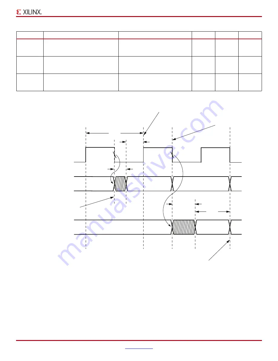
T

TSU

Target Setup Time
(TDI or TMS relative to the 
positive edge of TCK)

V

REF

 = 1.5V to 3.3V

4.8

ns

T

CSU

Cable Setup Time
(TDO relative to the 
negative edge of TCK)

V

REF

 = 1.5V to 3.3V

15.8

ns

T

TPD

Target Propagation Delay Time
(TDO relative to the
negative edge of TCK)

V

REF

 = 1.5V to 3.3V

24.6

ns

X-Ref Target - Figure 31

Notes: 

1.

All times are in nanoseconds and are relative to the target system interface connector.

2.

T

TSU

 Min is the minimum setup time guaranteed by Platform Cable USB II relative to the positive edge of TCK_CCLK_SCK.

3.

T

CSU

 Min is the minimum setup required by Platform Cable USB II to properly sample TDO_DONE_MISO.

4.

Propagation delays associated with buffers on the target system must be taken into account to satisfy the minimum setup times.

Figure 31:

Platform Cable USB II Timing Diagram

Table  10:

Switching Characteristics

Symbol

Description

Conditions

Min

Max

Units

Target devices samples TMS_PROG_SS and 
TDI_DIN_MOSI on the rising edge of TCK_CCLK_SCK

T

CLK

T

TSU

T

CPD

TCK_CCLK_SCK

TMS_PROG_SS /

TDI_DIN_MOSI

TDO_DONE_MISO

Platform Cable USB II asserts 

TMS_PROG_SS and 

TDI_DIN_MOSI on the falling 

edge of TCK_CCLK_SCK

T

TPD

Platform Cable USB II samples TDO_DONE_MISO 

on the falling edge of TCK_CCLK_SCK

T

CSU

Target device asserts TDO_DONE_MISO 
on the falling edge of TCK_CCLK_SCK

DS593_31_021408

Summary of Contents for Platform Cable USB II

Page 1: ...an and XC4000 FPGA families XC9500 XC9500XL XC9500XV and CoolRunner XPLA3 CoolRunner II CPLDs Note Xilinx iMPACT software is required for programming and configuration Third party PROM device programm...

Page 2: ...ACT download software using Boundary Scan IEEE 1149 1 IEEE 1532 Slave Serial mode or serial peripheral interface SPI Note iMPACT is bundled with Foundation ISE software and WebPACK ISE software In add...

Page 3: ...PCMCIA card Platform Cable USB II is designed to take full advantage of the bandwidth of USB 2 0 ports but it is also backward compatible with USB 1 1 ports Refer to USB Hub Types and Cable Performanc...

Page 4: ...ected by the host operating system Additional firmware can also be downloaded to the microcontroller once a design tool establishes a connection with the cable The USB protocol guarantees that the fir...

Page 5: ...Platform Cable USB II using the Xilinx iMPACT graphical user interface GUI For cable communication using other Xilinx design tools or methods please refer to the appropriate software user guide Selec...

Page 6: ...Configuration mode to Slave Serial mode or vice versa iMPACT can be disconnected from the cable using Output Cable Disconnect Figure 4 page 6 After the mode switch is complete reestablish the cable co...

Page 7: ...applications to uniquely identify and access a specific USB cable when multiple USB cables up to 127 are connected to the same host iMPACT provides a dialog box Figure 6 page 7 allowing users to selec...

Page 8: ...ign tools and iMPACT versions earlier than 7 1i do not restrict the TCK_CCLK_SCK selections in JTAG mode Accordingly users should take care to select a TCK_CCLK_SCK frequency matching the JTAG TCK spe...

Page 9: ...EF Users must design their system hardware with pin 2 attached to a voltage plane suppling the JTAG SPI or Slave Serial pins on the target device s Some devices have separate power pins for this purpo...

Page 10: ...Status LED LED Color LED State Condition OFF Continuous Host power OFF AMBER Continuous Target VREF 1 3V AMBER Blinking Target VREF 1 3V AND multiple cable identification active GREEN Continuous Targ...

Page 11: ...d Note This feature is not supported in earlier versions of iMPACT while iMPACT is operating in batch mode or by other Xilinx design tools In these cases it is recommended that suspend be disabled in...

Page 12: ...e unintentionally connected to high voltages The Xilinx product number for the flying wire set is HW USB FLYLEADS G X Ref Target Figure 10 Notes 1 Ribbon Cable 14 pin conductor 1 0 mm center round con...

Page 13: ...Mb s signaling should not be used with Platform Cable USB II A standard series B receptacle Figure 13 is incorporated into the case for mating with the detachable Hi Speed A B cable A separate chassis...

Page 14: ...e USB II ribbon cable X Ref Target Figure 14 Figure 14 Target Interface Connector Dimensions and Signal Assignments Table 5 Mating Connectors for 2 mm pitch 14 Conductor Ribbon Cable Manufacturer 1 SM...

Page 15: ...is idle Figure 16 page 16 shows a typical use of PGND as a control signal to manage a target system s JTAG chain PGND drives the select S term on a set of multiplexers that switch between the primary...

Page 16: ...oltages pins are connected to VCCAUX 5 Pin 13 is grounded on legacy Xilinx USB cables models DLC9 DLC9G and DLC9LP and Parallel Cable IV model DLC7 These cables need to be manually detached from the 2...

Page 17: ...for a hardware jumper to ground on the PROG_B signal and the need for additional control logic PGND is controlled by an open drain driver Note PGND control for SPI programming is available in iMPACT v...

Page 18: ...fferent pin names and requirements Refer to the SPI flash data sheet for the equivalent pins and device requirements 2 The example shows the interconnect and device requirements for a Xilinx Spartan 3...

Page 19: ...powered and attached to the target system while the target system power is off Bidirectional Signal Pins Platform Cable USB II provides five bidirectional signal pins TDI_DIN_MOSI TDO_DONE_MISO TCK_CC...

Page 20: ...ef Target Figure 19 Figure 19 VREF Current vs VREF Voltage X Ref Target Figure 20 Figure 20 Target Interface Driver Topology DS593_19_021408 FPGA NC7SZ126 Output High Z Control I O Pin 2 mm Connector...

Page 21: ...supply See Table 9 page 32 for VIL and VIH specifications The receive buffers can tolerate voltages higher than the bias voltage without damage compensating for target system drivers in multi device c...

Page 22: ...vides the option of enabling the HALT pin during JTAG operations Figure 24 This option is accessed by clicking on the Xilinx FPGA in the iMPACT GUI and selecting Edit Set Programming Properties to ope...

Page 23: ...O JTAG chains or MISO dedicated SPI in system programming when incorporating the 2 mm IDC connector In particular if an open drain or open collector buffer is inserted between TDO MISO and the cable t...

Page 24: ...11 ns is attributable exclusively to input delays in the cable At 12 MHz there is still sufficient setup time before the cable samples prior to the next negative TCK transition X Ref Target Figure 25...

Page 25: ...m 25 X Ref Target Figure 26 Figure 26 TDO Sampling Example at 12 MHz TDO Propagation Delay DS593_26_021408 Negative TCK transition at G1 causes target device to change TDO state which propagates to th...

Page 26: ...rch 17 2011 www xilinx com 26 X Ref Target Figure 27 Figure 27 TDO Sampling Example at 12 MHz TDO Setup Time Relative to Sampling Point DS593_27_011508 TDO setup time prior to internal sampling clock...

Page 27: ...in Figure 29 are followed Buffering is essential if target devices are distributed over a large PCB area Each differential driver and or receiver pair contributes approximately 5 ns of propagation de...

Page 28: ...for a single USB 1 1 full speed device However because hub bandwidth must be shared among all connected devices actual bandwidth is in practice lower than these theoretical values Platform Cable USB I...

Page 29: ...get ISP devices sharing the same data stream 8 TDO In JTAG Test Data Out This pin is the serial data stream received from the TDO pin on the last device in a JTAG chain 1 X Root Hub 12 Mb s Bus Speed...

Page 30: ...the target serial input data stream for SPI operations and should be connected to the D 1 pin on the SPI flash device 13 PGND Out SPI Pseudo Ground PGND is pulled Low during SPI operations otherwise i...

Page 31: ...the INIT_B pin of the target FPGA for a single device system or to the INIT_B pin on all FPGAs in parallel in a daisy chain configuration 3 5 7 9 11 Digital Ground All ground pins should be connected...

Page 32: ...n Max Units IREF Target Supply Current VREF 3 3V 15 mA VREF 2 5V 3 VREF 1 8V 1 VREF 1 5V 1 VOH High Level Output Voltage VREF 3 3V IOH 8 mA 2 25 V VREF 2 5V IOH 8 mA 2 15 VREF 1 8V IOH 8 mA 1 55 VREF...

Page 33: ...in nanoseconds and are relative to the target system interface connector 2 TTSU Min is the minimum setup time guaranteed by Platform Cable USB II relative to the positive edge of TCK_CCLK_SCK 3 TCSU M...

Page 34: ...nd if not installed and used in accordance with the data sheet could cause harmful interference to radio communications Operation of this equipment in a residential area is likely to cause harmful int...

Page 35: ...WITHOUT NOTICE PRODUCTS ARE NOT DESIGNED OR INTENDED TO BE FAIL SAFE OR FOR USE IN ANY APPLICATION REQUIRING FAIL SAFE PERFORMANCE SUCH AS LIFE SUPPORT OR SAFETY DEVICES OR SYSTEMS OR ANY OTHER APPLIC...

Reviews: