KC724 GTX Transceiver Characterization Board
43
UG932 (v2.2) October 10, 2014
Appendix A
Default Jumper and Switch Positions
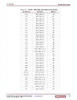
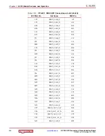
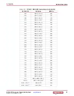
lists the jumpers that must be installed on the board for proper operation. These
jumpers must be installed except where specifically noted in this user guide. PCB
Assembly Drawing 0431643 shows the location and the default placement of all jumpers
on their respective connectors on the board.
Note:
Any jumper not listed in
should be left open for normal operation.
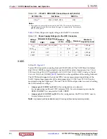
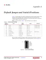
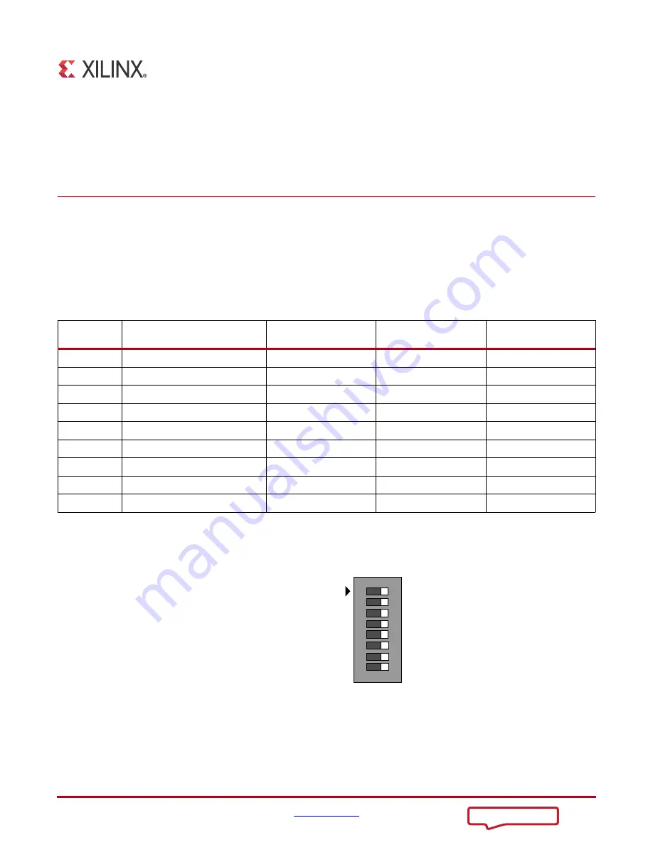
DIP switch SW10 enables the supply of onboard core power to the FPGA. For normal
operation positions 1 through 6 must be set to the ON position as shown in
.
Table A-1:
Default Jumper Settings
Reference
Designator
Name
Board
Location
Jumper
Comments
J48
<None>
Upper-left
CTRL (1–2)
UCD9248 reset pin
J49
<None>
Upper-left
CTRL (1–2)
UCD9248 reset pin
J50
<None>
Upper-left
CTRL (1–2)
UCD9248 reset pin
J4
UTIL_3V3
Upper-left
CTRL (1–2)
J24
UTIL_5V0
Upper-left
CTRL (1–2)
J78
VTT SOURCE
Upper-left
VTT
→
GND (1–2)
Red 20A jumper
J141
VCCADC SELECT
Upper-middle
VCCAUX (1–2)
J142
VREF SEL
Upper-middle
REG (1–2)
J140
PMBUS CTRL
Upper-right
ALWAYS ON (2-3)
X-Ref Target - Figure A-1
Figure A-1:
Default Switch Settings
SW10
1
234
5
NC
NC
VCCO_HR
VCCO_HP
VCCAUX_IO
ON
67
8
VCCBRAM
VCCAUX
VCCINT
Pin 1
UG932_aB_01_062812

