


28
FMC XM105 Debug Card User Guide
UG537 (v1.3) June 16, 2011
Chapter 1:
XM105
15. 2-Kb EEPROM
A ST Microelectronics M24C02 2-Kb serial IIC bus EEPROM component provides a small
amount of non-volatile memory storage on the XM105.
The IIC address of this component is controlled by a combination of the specific board
interface and chip enable connections to the component inputs on the XM105. Signals GA0
and GA1 from the board are connected to the chip enable inputs of the M24C02 component
enables E0 and E1. As shown in
, Xilinx boards provide GA0 and GA1 signal
strapping to 3.3V and GND signals, which creates a different E0 and E1 chip enable decode
on the E1 and E0 inputs of the EEPROM.
The IIC memory addressing protocol requires a bus master to initiate communication to a
peripheral device using a start condition followed by a device select code. The device select
code consists of a 4-bit Device Type Identifier and a 3-bit Chip Enable Address (E2, E1, E0).
Bit 0 is used to indicate read/write. The Device Type Identifier for the EEPROM is
1010
binary.
shows the generic EEPROM Device Select Code as well as specific
Device Code Select addresses for the EEPROM when the XM105 is connected to boards
defined in
.
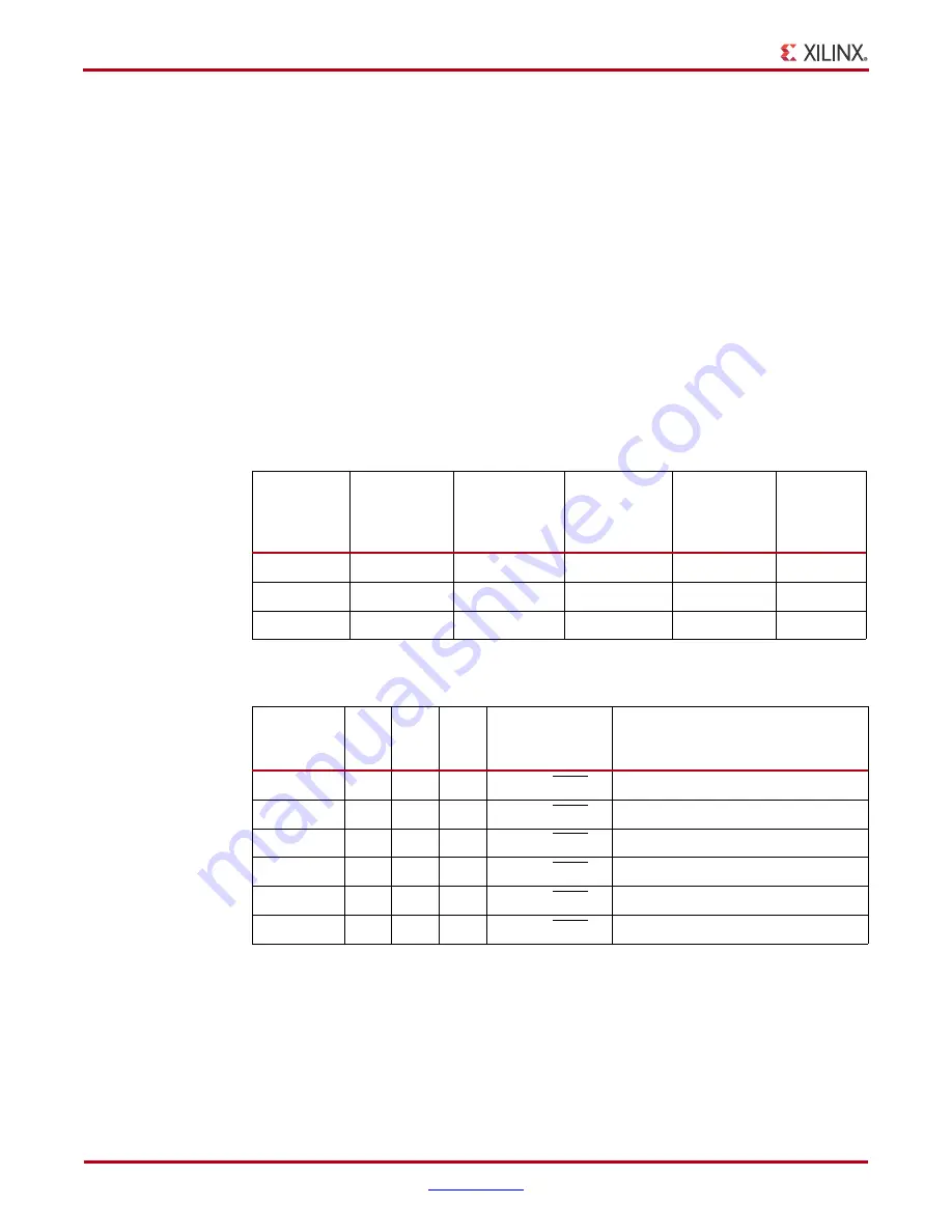
Table 1-16:
M24C02 Enable Input Connections
M24C02 Chip
Enable Input
FMC HPC
Control
Signal
Connection
SP601 LPC
Connector
SP605 LPC
Connector
ML605 LPC
Connector
ML605 HPC
Connector
E0
GA1
GND
GND
3.3V GND
E1
GA0
3.3V
3.3V
GND
GND
E2
GND
GND
GND
GND
GND
Table 1-17:
EEPROM IIC Device Select Code
Bit 7:4
Device Type
Identifier
Bit 3
Bit 2
Bit 1
Bit 0 (LSB)
Description
1010
E2
E1
E0
Read/Write
M24C02 Device Select Code
1010
0
GA0
GA1
Read/Write
Connected to XM105
1010
0
1
0
Read/Write
Connected to SP601 LPC interface
1010
0
1
0
Read/Write
Connected to SP605 LPC interface
1010
0
0
1
Read/Write
Connected to ML605 LPC interface
1010
0
0
0
Read/Write
Connected to ML605 HPC interface


