


12
FMC XM101 User Guide
UG538 (v1.1) September 24, 2010
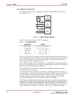
Chapter 1:
XM101
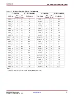
Table 1-2:
XM101 Features
Number
Feature
Notes
Schematic
Page
1
VITA 57.1 FMC
HPC connector
J1: 80 signal pairs comprised of LA[00:33],
HA[00:23] and HB[00:21], four clock pairs, and
the IIC bus SDA, SCL. The connector is mounted
on the bottom side of the card.
3 - 6
2
Samtec QSE
Connectors
P1-P4: 4 Samtec QSE connectors with length-
matched signal pairs wired to the FMC HPC
connector as follows: P1 QSE0 LA[00:16], P2
QSE1 LA[17:33], P3 QSE2 HA[00:23], P4 QSE3
HB[00:21].
7
3
PCA9543 IIC
Bus Switch
U4: IIC bus switch is connected to the main FMC
HPC IIC bus SDA and SCL signals. This
component can switch its input IIC bus to one of
two backside IIC bus connections. Each of the
two Si570 clock chips resides on one of these
backside IIC buses.
8
4
Silicon Labs
Si570
Programmable
XO/VCXO
U1, U2: Silicon Labs Si570 IIC serial bus
programmable clock source devices with
frequency range 10 MHz - 810 MHz. U1 drives
signals CLK0_M2C_P/N; U2 drives
CLK2_M2C_P/N
8
5
SMA Clock
Connections
SMA pair J2 and J3 are connected to
CLK1_M2C_P and N, respectively; SMA pair J4
and J5 are connected to CLK3_M2C_P and N,
respectively.
8
6
M24C02 2Kb IIC
EEPROM
U3: IIC compatible electrically erasable
programmable memory (EEPROM) with 2 Kb
(256 bytes) of non-volatile storage.
8
Summary of Contents for FMC XM101 LVDS QSE
Page 1: ...FMC XM101 LVDS QSE Card User Guide UG538 v1 1 September 24 2010 ...
Page 4: ...4 www xilinx com FMC XM101 User Guide UG538 v1 1 September 24 2010 ...
Page 6: ...6 www xilinx com FMC XM101 User Guide UG538 v1 1 September 24 2010 Preface About This Guide ...
Page 22: ...22 www xilinx com FMC XM101 User Guide UG538 v1 1 September 24 2010 Chapter 1 XM101 ...