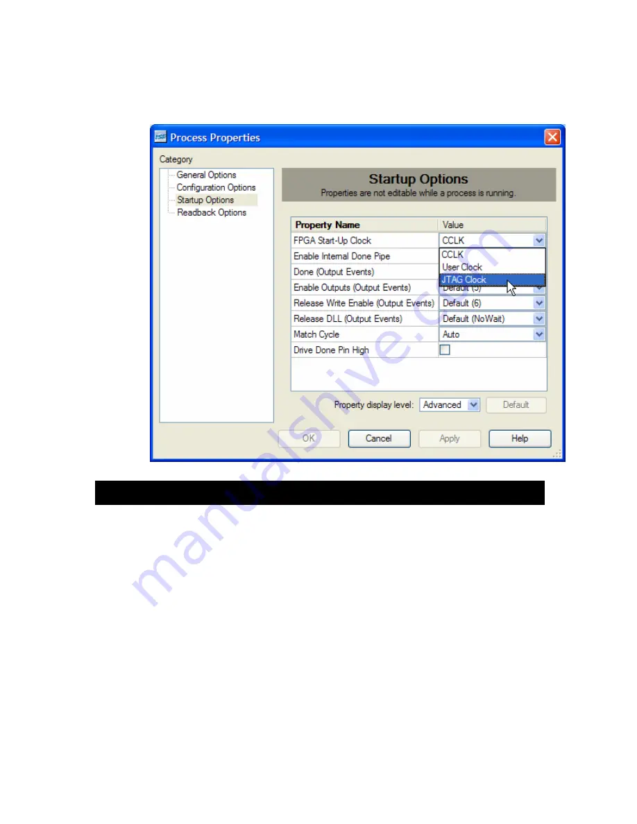
Then select the Startup Options tab in the Process Properties window and change the
FPGA Start-Up Clock to JTAG Clock. Then click on the OK button. After this option is set,
you can generate your bitstream and download it to the FPGA through the XSUSB Board.
FPGA Bitstream Generation Options When Using the Flash
Once your design is working correctly, you might want to store its bitstream in the
nonvolatile flash memory of your XSA or XSB Board so the FPGA will start to function as
soon as power is applied. In this case, you will need to change the FPGA Start-Up Clock
to the CCLK option and regenerate the bitstream (see the previous section for the steps to
do this). If you leave the FPGA Start-Up Clock as the JTAG Clock, then your design will
not startup correctly when it is transferred from the flash into the FPGA.
Once the bitstream is generated with the CCLK as the startup clock, you will need to use
the promgen utility to convert the .BIT file into a form that can be loaded into the flash on
your XSA or XSB Board. Please see the manual for your XSA or XSB Board for the exact
conversion procedure.
XSUSB INTERFACE BOARD V1.0 USER MANUAL
11


