FOR MOBILE APPLICATIONS
W25Q256FV
Publication Release Date: May 13, 2012
- 96 - Preliminary - Revision M1
9.7
AC Electrical Characteristics (
cont’d)
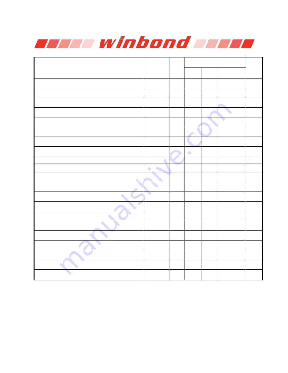
DESCRIPTION SYMBOL
ALT
SPEC
UNIT
MIN TYP MAX
/HOLD
Active Hold Time relative to CLK
t
CHHH
5
ns
/HOLD
Not Active Setup Time relative to CLK
t
HHCH
5
ns
/HOLD
Not Active Hold Time relative to CLK
t
CHHL
5
ns
/HOLD
to Output Low-Z
t
HHQX
(2)
t
LZ
7
ns
/HOLD
to Output High-Z
t
HLQZ
(2)
t
HZ
12
ns
Write Protect Setup Time Before /CS Low
t
WHSL
(3)
20
ns
Write Protect Hold Time After /CS High
t
SHWL
(3)
100
ns
/CS High to Power-down Mode
t
DP
(2)
3 µs
/CS High to Standby Mode without ID Read
t
RES
1
(2)
3
µs
/CS High to Standby Mode with ID Read
t
RES
2
(2)
1.8
µs
/CS High to next Instruction after Suspend
t
SUS
(2)
20 µs
/CS High to next Instruction after Reset
t
RST
(2)
30 µs
/RESET pin Low period to reset the device
t
RESET
(2)
1
(5)
µs
Write Status Register Time
t
W
10 15 ms
Byte Program Time (First Byte)
(4)
t
BP1
30 50 µs
Additional Byte Program Time (After First Byte)
(4)
t
BP2
2.5 12 µs
Page Program Time
t
PP
0.7 3 ms
Sector Erase Time (4KB)
t
SE
100
400 ms
Block Erase Time (32KB)
t
BE
1
120
1,600
ms
Block Erase Time (64KB)
t
BE
2
150
2,000
ms
Chip Erase Time
t
CE
80 400 s
Notes:
1.
Clock high + Clock low must be less than or equal to 1/f
C
.
2.
Value guaranteed by design and/or characterization, not 100% tested in production.
3.
Only applicable as a constraint for a Write Status Register instruction when SRP[1:0]=(0,1).
4.
For multiple bytes after first byte within a page,
t
BPN
=
t
BP1
+
t
BP2
*
N
(typical) and
t
BPN
=
t
BP1
+
t
BP2
*
N
(max), where N =
number of bytes programmed.
5.
It is possible to reset the device with shorter tRESET (as short as a few hundred ns), a 1us minimum is recommended to
ensure reliable operation.
6.
Tested on sample basis and specified through design and characterization data. TA = 25° C, VCC = 3.0V, 100% driver
strength.