CONFIDENTIAL – DO NOT COPY
Page 8-
12
File No. SG-0184
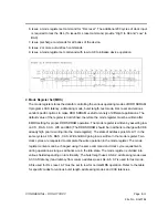
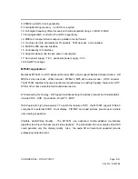
6. Issue a mode register set command for “DLL reset”. The additional 200 cycles of clock input
is required to lock the DLL.(To issue DLL reset command, provide “High” to A8 and “Low” to
BA0)
7. Issue precharge commands for all banks of the device.
8. Issue 2 or more auto-refresh commands.
9. Issue a mode register set command with low to A8 to initialize device operation.
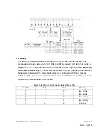
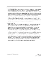
2. Mode Register Set (MRS)
The mode register stores the data for controlling the various operating modes of DDR SDRAM.
It programs CAS latency, addressing mode, burst length, test mode, DLL reset and various
vendor specific options to make DDR SDRAM useful for variety of different applications. The
default value of the register is not defined, therefore the mode register must be written after
EMRS setting for proper DDR SDRAM operation. The mode register is written by asserting low
on CS , RAS , CAS , WE and BA0 (The DDR SDRAM should be in all bank recharge with CKE
already high prior to writing into the mode register). The state of address pins A0~A11 in the
same cycle as CS , RAS , CAS , WE and BA0 going low is written in the mode register. Two
clock cycles are requested to complete the write operation in the mode register. The mode
register contents can be changed using the same command and clock cycle requirements
during operation as long as all banks are in the idle state. The mode register is divided into
various fields depending on functionality. The burst length uses A0~A2, addressing mode uses
A3, CAS latency (read latency from column address) uses A4~A6. A7 is used for test mode.
A8 is used for DLL reset. A7 must be set to low for normal MRS operation. Refer to the table
for specific codes for various burst length, addressing modes and CAS latencies.
Summary of Contents for VIZIO P42HDTV10A
Page 1: ......
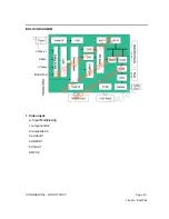
Page 27: ...CONFIDENTIAL DO NOT COPY Page 6 3 File No SG 0184 Main Board Block Diagram ...
Page 60: ...CONFIDENTIAL DO NOT COPY Page 8 28 File No SG 0184 ...
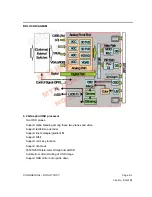
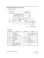
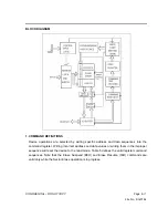
Page 61: ...CONFIDENTIAL DO NOT COPY Page 8 29 File No SG 0184 BLOCK DIAGRAM ...
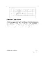
Page 68: ...CONFIDENTIAL DO NOT COPY Page 8 36 File No SG 0184 Fig D READ TIMING WAVEFORMS ...
Page 69: ...CONFIDENTIAL DO NOT COPY Page 8 37 File No SG 0184 Fig E RESET TIMING WAVEFORM ...
Page 72: ...CONFIDENTIAL DO NOT COPY Page 8 40 File No SG 0184 Pin Configuration 400mil TSOP II x4 x8 x16 ...
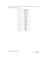
Page 94: ...CONFIDENTIAL DO NOT COPY Page 9 2 File No SG 0184 3 5V DV50A CB15 4 3 3V DV33A U5 3 ...
Page 95: ...CONFIDENTIAL DO NOT COPY Page 9 3 File No SG 0184 5 2 5V DV25 CE42 6 1 8V DV18A U5 2 ...
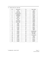
Page 100: ...CONFIDENTIAL DO NOT COPY Page 9 8 File No SG 0184 3 3 3V DV33 C11 4 2 5V DV25 C185 ...
Page 101: ...CONFIDENTIAL DO NOT COPY Page 9 9 File No SG 0184 5 1 8V DV18 C64 6 1 25V 1V25_DDR C148 ...
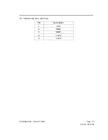
Page 102: ...CONFIDENTIAL DO NOT COPY Page 9 10 File No SG 0184 7 1 2V DV12 C26 ...
Page 111: ...CONFIDENTIAL DO NOT COPY Page 10 7 File No SG 0184 TROUBLE OF THE DTV ...
Page 196: ......
Page 197: ......
Page 198: ......
Page 199: ......
Page 200: ......
Page 201: ......
Page 202: ...CAM Products 2000 TM smbot art bot art ...
Page 203: ...C ...
Page 204: ...C ...
Page 205: ...CAM350 V 7 6 Tue Feb 07 05 50 42 2006 Untitled VCC SCH ...
Page 206: ...CAM350 V 7 6 Tue Feb 07 05 50 48 2006 Untitled Board ...
Page 207: ...CAM350 V 7 6 Tue Feb 07 05 50 50 2006 Untitled BotSilk ...
Page 208: ...CAM350 V 7 6 Tue Feb 07 05 50 51 2006 Untitled GND ...
Page 209: ...CAM350 V 7 6 Tue Feb 07 05 50 53 2006 Untitled Board ...
Page 210: ...CAM350 V 7 6 Tue Feb 07 05 50 54 2006 Untitled TopSilk ...
Page 211: ...CAM350 V 7 6 Tue Feb 07 05 50 55 2006 Untitled VCC ...
Page 212: ......
Page 213: ......
Page 214: ......
Page 215: ......
Page 216: ......
Page 217: ......
Page 218: ......
Page 219: ......

