background image


LENA-R8 series - System integration manual 

UBX-22015376 - R02 

System description


Page 8 of 116 

C1-Public 


1.3


Architecture 

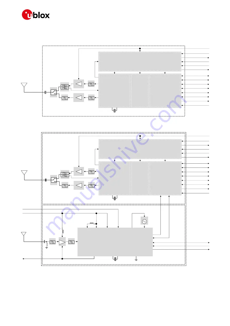
Figure 1

 summarizes the internal architecture of the LENA-R8001 modules. 

UARTs
USB

VCC

V_BCKP

RF 

Transceiver

Flash 

Memory

Base Band

Processor

26 MHz 

32 kHz 

V_INT
PWR_ON
RESET_N

SIM
I2C
Digital Audio
GPIOs
Antenna Tuner

USB boot

Power 

Management

ANT_DET

ANT

Power

Amplifiers

Duplexer

Filters

Switch

Power

Amplifiers

Filters

Filters

Filters


Figure 1: LENA-R8001 modules simplified block diagram 

Figure 2

 summarizes the internal architecture of the LENA-R8001M10 modules. 

ANT_GNSS

UARTs
USB

LNA

UBX-M10050

LNA_EN

RF_IN

V_BCKP

26 MHz

VCC

RTC

VIO_SEL

EXTINT
TIMEPULSE

TCXO

ANT_ON

Time-Pulse

Ext-Int

Tx-Ready

I2C

UART

UART_GNSS

V_BCKP

VBCKP_GNSS

VCC_GNSS

LDO_X_OUT

RF 

Transceiver

32 kHz 

V_CORE

V_IO

V_RF

Flash 

Memory

Base Band

Processor

26 MHz 

32 kHz 

V_INT
PWR_ON
RESET_N

SIM
I2C
Digital Audio
GPIOs
Antenna Tuner

USB boot

Power 

Management

GNSS 

System

Cellular 

System

ANT_DET

ANT

Power

Amplifiers

Duplexer

Filters

Switch

Power

Amplifiers

Filters

Filters

Filters

SAW

SAW


Figure 2: LENA-R8001M10 modules simplified block diagram 


The “00

C

” product versions of the 

LENA-R8 series modules (meaning the LENA-R8001-00C and 

the LENA-R8001M10-00C versions) do not support the antenna tuner interface on the 

RFCTRL1 

and 

RFCTRL2

 pins, which are intended to be left unconnected 

Summary of Contents for LENA-R8 Series

Page 1: ...r GSM GPRS bands these modules offer universal network connectivity and global coverage The integrated GNSS receiver based on the u blox M10 platform make the modules ideal for demanding global tracki...

Page 2: ...of life Production information Document contains the final product specification This document applies to the following products Product name Type number Modem version Application version PCN referenc...

Page 3: ...tem reset 23 1 8 Cellular antenna interface 23 1 8 1 Cellular antenna RF interface ANT 23 1 8 2 Cellular antenna detection ANT_DET 24 1 8 3 Cellular antenna dynamic tuning interface RFCTRL1 RFCTRL2 25...

Page 4: ...ar antenna detection interface ANT_DET 64 2 4 6 Cellular antenna dynamic tuning interface RFCTRL1 RFCTRL2 66 2 5 Cellular SIM interface 67 2 6 Cellular serial communication interfaces 74 2 6 1 Cellula...

Page 5: ...provals 103 4 1 Product certification approval overview 103 4 2 US Federal Communications Commission notice 104 4 2 1 Safety warnings review the structure 104 4 2 2 Declaration of conformity 104 4 2 3...

Page 6: ...S GLONASS Galileo BeiDou The cellular modem and GNSS subsystems are accessible via dedicated interfaces for large usage flexibility Both subsystems can be operated fully independently facilitating the...

Page 7: ...M10 standard precision receiver with concurrent reception of up to four GNSS LTE bands FDD band 12 700 MHz FDD band 28 700 MHz FDD band 20 800 MHz FDD band 5 850 MHz FDD band 8 900 MHz FDD band 4 170...

Page 8: ...ANT_GNSS UARTs USB LNA UBX M10050 LNA_EN RF_IN V_BCKP 26 MHz VCC RTC VIO_SEL EXTINT TIMEPULSE TCXO ANT_ON Time Pulse Ext Int Tx Ready I2C UART UART_GNSS V_BCKP VBCKP_GNSS VCC_GNSS LDO_X_OUT RF Transce...

Page 9: ...only The GNSS receiver system of LENA R8001M10 modules is composed of the following main elements u blox UBX M10050 KB concurrent GNSS chipset with SPG 5 10 FW version Dedicated supply main input VCC...

Page 10: ...ce Antenna circuit affects the RF performance and compliance of the device integrating the module with applicable required certification schemes See section 1 8 for description and requirements See se...

Page 11: ...1 for functional description See section 2 6 1 for external circuit design in DTR 9 I Cellular UART data terminal ready input 1 8 V input UART Circuit 108 2 DTR per ITU T V 24 Internal active pull up...

Page 12: ...tion See section 2 6 2 for external circuit design in USB_D 29 I O USB Data Line D USB interface supporting AT data communication FOAT GNSS tunneling FW update by dedicated tool diagnostic 90 nominal...

Page 13: ...ircuit design in GNSS PIOs TIMEPULSE 45 O GNSS time pulse LENA R8001M10 only GNSS time pulse output function See section 1 18 for functional description See section 2 12 for external circuit design in...

Page 14: ...in active mode The available communication interfaces are ready the cellular system can accept and respond to AT commands entering connected mode upon cellular RF signal reception transmission LENA R...

Page 15: ...receiver demonstrates di erent behavior In on o operation the receiver switches between phases of startup navigation and phases with low or almost no system activity backup sleep In cyclic tracking th...

Page 16: ...R8 series modules must be supplied via the three VCC pins that represent the cellular system power supply input The VCC pins are internally connected to the RF power amplifier and to the integrated P...

Page 17: ...wn in the LENA R8 series data sheet 1 See 1 6 1 3 1 6 1 2 for connected mode current profiles VCC peak current Support with margin the highest peak VCC current consumption value in connected mode cond...

Page 18: ...rame 8 slots burst so with a 1 8 duty cycle according to GSM TDMA Time Division Multiple Access If the module is transmitting in 2G single slot mode in the 1800 or 1900 MHz bands the current consumpti...

Page 19: ...gure 8 VCC current consumption profile with power saving enabled and module registered with the network the module is in low power idle mode and periodically wakes up to active mode to monitor the pag...

Page 20: ...ENA R8 series interfaces supply output V_INT simplified block diagram 1 7 Cellular system function interfaces 1 7 1 Cellular system power on When LENA R8 series modules cellular system is not powered...

Page 21: ...at the cellular system is ready to operate Before the switch on of the generic digital interface supply V_INT of the module no voltage driven by an external application should be applied to any generi...

Page 22: ...T interface the switch off routine is in progress At the end of the switch off routine all the digital pins are tri stated and all the internal voltage regulators are turned off including the generic...

Page 23: ...module by forcing a low level on the RESET_N input see LENA R8 series data sheet 1 RESET_N low time to trigger cellular system reset during cellular system normal operation the RESET_N line should be...

Page 24: ...e to comply with the Over The Air OTA radiated performance requirements as the Total Radiated Power TRP and the Total Isotropic Sensitivity TIS specified by the applicable related certification scheme...

Page 25: ...9 2 Cellular SIM card detection interface The GPIO5 pin is configured by default to detect the external SIM card mechanical physical presence The pin is configured as input and it can sense SIM card p...

Page 26: ...ons and interprets all the characters received as commands to execute All supported functionalities can be configured by the AT commands documented in the AT commands manual 2 Hardware flow control is...

Page 27: ...during the firmware update over the USB interface Proper precaution must be taken for the DSR line if it is connected to an output of an external device or if it is grounded Use for example an extern...

Page 28: ...thernet over USB capability in addition to the vendor specific virtual serial ports listed above with change in the USB PID The USB interface is compatible with standard Linux Android USB kernel drive...

Page 29: ...frame length 1 12 Cellular clock output LENA R8 series modules cellular system provides digital clock output functionality on the GPIO6 pin This is mainly designed to feed the clock input of an exter...

Page 30: ...ruption at the main VCC_GNSS input pin Connecting an external DC power supply at the VBCKP_GNSS input is optional If present it enables the hardware backup mode when the main VCC_GNSS supply is not pr...

Page 31: ...about GNSS UART interface see the u blox M10 standard precision GNSS chip data sheet 3 integration manual 4 and interface description 5 It is recommended to provide access to the RXD_GNSS and TXD_GNS...

Page 32: ...D and VUSB_DET pins Accurate design is required to ensure USB 2 0 high speed interface functionality Carefully follow the suggestions provided in the related section 2 6 2 for schematic and layout des...

Page 33: ...han 5 V than the modules VCC operating supply voltage The use of switching step down provides the best power efficiency for the overall application and minimizes current drawn from the main supply sou...

Page 34: ...arge capacitance and very low ESR placed close to the module VCC pins Depending on the actual capability of the selected regulator or battery the required capacitance can be considerably larger than 1...

Page 35: ...ND Figure 18 Example of high reliability VCC supply application circuit using a step down regulator Reference Description Part number manufacturer C1 10 F Capacitor Ceramic X7R 5750 15 50 V C5750X7R1H...

Page 36: ...met C3 5 6 nF Capacitor Ceramic X7R 0402 10 50 V GRM155R71H562KA88 Murata C4 6 8 nF Capacitor Ceramic X7R 0402 10 50 V GRM155R71H682KA88 Murata C5 56 pF Capacitor Ceramic C0G 0402 5 50 V GRM1555C1H560...

Page 37: ...ample of a high reliability power supply circuit where the VCC module supply is provided by an LDO linear regulator capable of delivering the specified highest peak pulse current with the proper power...

Page 38: ...nufacturers U1 LDO Linear Regulator ADJ 3 0 A LP38501ATJ ADJ NOPB Texas Instrument Table 11 Components for a low cost VCC supply application circuit using an LDO linear regulator See the section 2 2 1...

Page 39: ...abilities and proper DC series resistance is directly connected to the VCC supply input of the module Battery charging is completely managed by the STMicroelectronics L6924U Battery Charger IC that fr...

Page 40: ...lication device integrates an internal antenna 2 2 1 7 Guidelines for external charging and power path management circuit Application devices where both a permanent primary supply charging source e g...

Page 41: ...ority then the integrated switching charger will take the remaining current to charge the battery Additionally the power path control allows an internal connection from the battery to the module with...

Page 42: ...tion CG0402MLE 18G Bourns D3 Schottky Diode 40 V 3 A MBRA340T3G ON Semiconductor R1 R3 R5 R7 10 k Resistor 0402 1 1 16 W Various manufacturers R2 1 05 k Resistor 0402 1 0 1 W Various manufacturers R4...

Page 43: ...d can be properly placed on the VCC line for additional RF noise filtering in particular if the application device integrates an internal antenna Ferrite bead specifically designed for EMI noise suppr...

Page 44: ...an be implemented for specific e g battery powered applications considering that the voltage at the VCC pins 52 and 53 can drop to a value lower than the one at the VCC pin 51 keeping the module still...

Page 45: ...rops Adequate maximum Drain current see LENA R8 series data sheet 1 for module consumption Low leakage current to minimize the consumption C3 GND C2 C1 C4 LENA R8 series 52 VCC 53 VCC 51 VCC VCC suppl...

Page 46: ...switching DC DC converter place the large capacitor close to the DC DC output and minimize the VCC track length Otherwise consider using separate large capacitors for the DC DC converter and the cellu...

Page 47: ...e GND areas of all the multiple PCBs Good grounding of GND pins also ensures thermal heat sink This is critical during call connection when the real network commands the module to transmit at maximum...

Page 48: ...s Supply external voltage translators to connect the 1 8 V digital interfaces of the module cellular system to an external 3 0 V device see section 2 6 1 2 6 3 2 7 1 for more details Pull up I2C inter...

Page 49: ...n and an open drain output of an application processor Reference Description Part number manufacturer ESD Varistor array for ESD protection CT0402S14AHSG EPCOS Table 18 Example of pull up resistor and...

Page 50: ...st It is recommended to keep the connection line to RESET_N as short as possible 2 4 Antenna interfaces LENA R8 series modules provide an RF interface for connecting the external cellular antenna the...

Page 51: ...d plane by a dielectric material or a strip line consists of a flat strip of metal which is sandwiched between two parallel ground planes within a dielectric material The micro strip implemented as a...

Page 52: ...layers below any pad of component present on the RF transmission line if top layer to buried layer dielectric thickness is below 200 m to reduce parasitic capacitance to ground The transmission line w...

Page 53: ...e connectors require GND keep out i e clearance a void area on all the layers around the central pin up to annular pads of the four GND posts as shown in Figure 35 o U FL surface mounted connectors re...

Page 54: ...l dimensions of the application board are under analysis decision since the RF compliance of the device integrating LENA R8 series modules with all the applicable required certification schemes depend...

Page 55: ...equired certification schemes It is recommended to consult the antenna manufacturer for the design in guidelines for antenna matching relative to the custom application In both cases independently of...

Page 56: ...MHz 3300 5000 MHz 5150 5925 MHz 40 0 x 8 0 x 3 0 mm 2J Antennas 2JE38 Wideband cellular LTE surface mount fiberglass antenna 698 960 MHz 1710 2170 MHz 2500 2700 MHz 40 0 x 7 0 x 3 0 mm Table 20 Examp...

Page 57: ...59 2 x 13 6 mm Taoglas GSA 8827 A 101111 Phoenix Wideband adhesive mount antenna with cable and SMA M 698 960 MHz 1575 42 MHz 1710 2700 Mhz 105 x 30 x 7 7 mm Taoglas TG 55 8113 LTE terminal mount mono...

Page 58: ...nal external circuitry 2 4 3 1 Guidelines for applications with a passive antenna If a GNSS passive antenna with high gain and good sky view is used together with a short 50 line between antenna and r...

Page 59: ...by another SAW filter before the u blox GNSS chipset as illustrated in Figure 2 The addition of such external components should be carefully evaluated especially in case the application power consump...

Page 60: ...S GLONASS Galileo BeiDou Taoglas CGGBP 35 3 A 02 Ceramic patch antenna GPS SBAS QZSS GLONASS Galileo BeiDou Taoglas CGGBP 18 4 A 02 Embedded patch antenna GPS SBAS QZSS GLONASS Galileo BeiDou Inpaq PA...

Page 61: ...esistor 0 5W Various manufacturers Table 27 Example component values for active antenna biasing Refer to the antenna datasheet and or manufacturer for proper values of the supply voltage VCC_ANT induc...

Page 62: ...erformance is particularly important in the scenarios where several radios of various forms are used in close proximity to each other 0 1 20 60 1 575 Frequency MHz Power dBm Filter gain dB 1 800 2025...

Page 63: ...ce again the C No Countermeasures against out of band interference include maintaining a good grounding concept in the design keeping the GNSS and cellular antennas more than the quarter wavelength of...

Page 64: ...SS RF coexistence it has to be noted that high power transmission occurs very infrequently typical values are in the range of 3 to 0 dBm see the Tx Power distribution in the GSMA TS 09 17 Therefore de...

Page 65: ...the ANT pins C2 and at the antenna radiating element C3 to decouple the DC current generated by the ANT_DET pin Choke inductors with a Self Resonance Frequency SRF in the range of 1 GHz are needed in...

Page 66: ...n be left unconnected and the ANT pin can be directly connected to the related antenna connector by a 50 transmission line as described in Figure 35 2 4 5 2 Guidelines for ANT_DET layout design The re...

Page 67: ...l the information needed to identify and authenticate subscribers over the cellular network Removable UICC SIM card contacts mapping is defined by ISO IEC 7816 and ETSI TS 102 221 as follows Contact C...

Page 68: ...SIM_CLK Case pin 5 UICC contact C4 AUX1 Aux contact It must be left not connected Case pin 1 UICC contact C5 GND Ground It must be connected to GND Case pin 2 UICC contact C6 VPP SWP Other It can be...

Page 69: ...capacitance i e less than 10 pF ESD protection e g Littelfuse PESD0402 140 on each externally accessible SIM line close to each related pad of the SIM connector the ESD sensitivity rating of the SIM i...

Page 70: ...pF to 47 pF e g Murata GRM1555C1H470J on each SIM line VSIM SIM_CLK SIM_IO SIM_RST to prevent RF coupling especially in case the RF antenna is placed closer than 10 30 cm from the SIM card holder Limi...

Page 71: ...SIM_RST very close to each related pad of the SIM connector to prevent RF coupling especially in case the RF antenna is placed closer than 10 30 cm from the SIM card holder Provide a low capacitance...

Page 72: ...IM switch to ensure high speed data transfer according to SIM requirements Connect the contacts C1 VCC of the two UICC SIM to the VSIM pin of the module by means of a proper 2 throw analog switch e g...

Page 73: ...etection not implemented 2 5 1 2 Guidelines for SIM layout design The layout of the SIM card interface lines VSIM SIM_CLK SIM_IO SIM_RST may be critical if the SIM card is placed far away from the LEN...

Page 74: ...24 link in DTE DCE serial communication 1 8 V DTE If a 3 0 V Application Processor DTE is used then it is recommended to connect the 1 8 V UART interface of the module DCE by means of appropriate uni...

Page 75: ...V 24 link in the DTE DCE serial communication 1 8 V DTE If a 3 0 V Application Processor DTE is used then it is recommended to connect the 1 8 V UART interface of the module DCE by means of appropria...

Page 76: ...slators on the module side as in Figure 54 4 V_INT TxD Application Processor 3 0V DTE RxD RTS CTS TxD RxD RTS CTS GND LENA R8 series 1 8V DCE 12 TXD UART data input 9 DTR AUX UART data input 13 RXD UA...

Page 77: ...ould be implemented as in Figure 55 TxD Application Processor 1 8V DTE RxD RTS CTS DTR DSR RI DCD GND LENA R8 series 1 8V DCE 12 TXD 9 DTR 13 RXD 10 RTS 11 CTS 6 DSR 7 RI 8 DCD GND 0 TP 0 TP Figure 55...

Page 78: ...l input 11 CTS UART flow ctrl output 8 DCD AUX UART data ouput 6 DSR AUX UART flow ctrl input 7 RI AUX UART flow ctrl output GND 0 TP 0 TP UART1 UART2 0 TP 0 TP 100 Figure 57 2 UART interfaces applica...

Page 79: ...of the resistance value for the external pull up biased by the application processor supply rail Do not apply voltage to any UART interface pin before the switch on of the UART supply source V_INT to...

Page 80: ...for USB application circuits If the USB interface pins are not used they can be left unconnected on the application board but it is highly recommended to provide accessible Test Points directly connec...

Page 81: ...and other external I2C bus devices as an audio codec Beside the general considerations explained below see the following parts of this section 2 6 3 1 for guidelines to connect external u blox GNSS r...

Page 82: ...related output bypass capacitor See GNSS receiver Hardware Integration Manual Table 43 Components for connecting LENA R8001 modules to u blox 1 8 V GNSS receivers Figure 63 illustrates an alternative...

Page 83: ...blox 3 0 V GNSS receiver providing the GNSS supply enable function A pull down resistor is provided to avoid a switch on of the positioning receiver when the cellular module is switched off The 1 8 V...

Page 84: ...nment synch signal frequency The same serial clock frequency 16 x 2 x 8 kHz Compatible voltage levels 1 80 V typ otherwise it is recommended to connect the 1 8 V digital audio interface of the module...

Page 85: ...Codec DACDAT ADCDAT SDA SCL MCLK C4 C2 C1 1V8 1V8 MICBIAS C17 R3 C5 C6 INN INP D1 Microphone Connector MIC C12 C11 J1 R4 C8 C7 D2 SPK Speaker Connector LOUTP LOUTN J2 C10 C9 C14 C13 EMI3 EMI4 EMI1 EM...

Page 86: ...he module VCC supply line any switching regulator line RF antenna lines digital lines and any other possible noise source Avoid coupling between the microphone and speaker receiver lines Optimize the...

Page 87: ...e GPIO5 pin see Figure 47 Table 35 in section 2 5 LENA R8 series GPIO1 R1 R3 3V8 Network Indicator R2 16 DL1 T1 Figure 66 Application circuit for network indication provided over GPIO1 Reference Descr...

Page 88: ...F Figure 67 Application circuit for LENA R8001M10 modules GNSS system supply using external 1 8 V supply system Do not add series resistance greater than 0 2 along the VCC_GNSS supply line to avoid vo...

Page 89: ...a load switch MOS transistor with very low on resistence keeping the series resistance lower than 0 2 along the VCC_GNSS supply line to avoid voltage ripple due to the dynamic current conditions 2 10...

Page 90: ...Test Point 1V8 B1 A1 GND U1 B2 A2 VCCB VCCA C1 C2 3V0 DIR1 DIR2 OEn 99 VCC_GNSS Unidirectional Voltage Translator Figure 70 Application circuit for LENA R8001M10 GNSS UART with 3 V external host appli...

Page 91: ...be driven by an external host processor If driving the GNSS UART pins cannot be avoided buffers are required for isolating the GNSS UART pins For more information and examples about GNSS PIOs external...

Page 92: ...production process requirements Foot print Top View K M1 M1 M2 E H J E B K G H J D A D O O L N L I F1 F2 G H G G ANT Pin 1 J Paste mask Top View K M1 M1 M2 E H J E B K G H J D A D O O L N L I F1 F2 G...

Page 93: ...characteristics mechanical shells enclosure or forced air flow The increase of the thermal dissipation i e the reduction of the Module to Ambient thermal resistance will decrease the temperature of th...

Page 94: ...llular Antenna 33pF ANT 8 2pF 24 GPIO3 V_INT B A GND VCCB VCCA SN74LVC1T45 Voltage Translator 100nF 100nF 3V0 TxD 4 7k IN OUT LDO Regulator SHDNn 4 7k 3V8 3V0 23 GPIO2 SDA_A SDA_B GND SCL_A SCL_B VCCA...

Page 95: ...D 1k TP V_INT VBUS 17 VUSB_DET 100nF 62 RSVD 82nH 59 ANT_DET 10k 27pF ESD 56 Connector Cellular Antenna 33pF ANT 8 2pF 24 GPIO3 23 GPIO2 GPIO4 25 4 7k 4 7k 0 TP 0 TP 0 TP 15pF 39nH Optional 0 otherwis...

Page 96: ...UART interfaces signals direction as the modules signal names follow the ITU T V 24 Recommendation 7 TXD is the module UART data input RXD is the module UART data output Capacitance and series resista...

Page 97: ...ation board providing a dense line of vias at the edges of each ground area in particular along the RF and high speed lines Keep routing short and minimize parasitic capacitance on the SIM lines to pr...

Page 98: ...tic Protective Area EPA The EPA can be a small working station or a large manufacturing area The main principle of an EPA is that there are no highly charging materials near ESD sensitive electronics...

Page 99: ...nd all parts will be heated up evenly regardless of material properties thickness of components and surface color Consider the IPC 7530A Guidelines for temperature profiling for mass soldering reflow...

Page 100: ...e 1 00 Soldering Profile 50 50 Elapsed time s Figure 76 Recommended soldering profile LENA R8 series modules must not be soldered with a damp heat process 3 3 3 Optical inspection After soldering the...

Page 101: ...lready populated on it Performing a wave soldering process on the module can result in severe damage to the device u blox gives no warranty against damages to the LENA R8 series modules caused by perf...

Page 102: ...icient to provide optimum immunity to interferences and noise u blox gives no warranty for damages to the LENA R8 series modules caused by soldering metal cables or any other forms of metal strips dir...

Page 103: ...tes a LENA R8 series module differ depending on the country or the region where the integrating device is intended to be deployed on the relative vertical market of the device on type features and fun...

Page 104: ...le certification filing The gain of the system antenna s used for the modules i e the combined transmission line connector cable losses and radiating element gain must not exceed the value specified i...

Page 105: ...nce of 20 cm between the radiator and the body of the user or nearby persons This transmitter must not be co located or operating in conjunction with any other antenna or transmitter except as authori...

Page 106: ...t conforme aux normes canadiennes CAN ICES 3 B NMB 3 B et CNR 210 Son fonctionnement est soumis aux deux conditions suivantes o cet appareil ne doit pas causer d interf rence o cet appareil doit accep...

Page 107: ...equency radiation exposure information this equipment complies with radiation exposure limits prescribed for an uncontrolled environment for fixed and mobile use conditions This equipment should be in...

Page 108: ...d Safety Article 6 1a o EN 62368 1 o EN 62311 Radiofrequency radiation exposure information this equipment complies with radiation exposure limits prescribed for an uncontrolled environment for fixed...

Page 109: ...ce of the design with RF regulatory rules defined by the FCC ISED RED etc can be verified using a radio communication tester callbox as for example the Rohde Schwarz CMW500 or any equivalent equipment...

Page 110: ...supported bands such as frequency tuning calibration of transmitter and receiver power levels etc Verification of RF characteristics after calibration such as modulation power levels spectrum etc are...

Page 111: ...y to test the GNSS RF functionality is with the use of a Multi GNSS signal generator as it assures reliable and constant signals at every measurement u blox recommends the Spirent GSS6300 Multi GNSS s...

Page 112: ...ter ANATEL Ag ncia Nacional de Telecomunica es National Telecommunications Agency Brazil APAC Asia Pacific ASIC Application Specific Integrated Circuit AT AT Command Interpreter Software Subsystem ATE...

Page 113: ...F Global Certification Forum GERA GSM EGPRS Radio Access GITEKI Gijutsu kijun tekig sh mei technical standard conformity certification Japan GLONASS Russian GLObal Navigation Satellite System GMSK Gau...

Page 114: ...mum Permissible Exposure MQTT Message Queuing Telemetry Transport MSB Most Significant Bit MSD Moisture Sensitive Device MUX Multiplexer N A Not Applicable NCC National Communications Commission Taiwa...

Page 115: ...lex TDMA Time Division Multiple Access THT Through Hole Technology TI Texas Instruments TIS Total Isotropic Sensitivity TLS Transport Layer Security TP Test Point TRP Total Radiated Power TTFF Time To...

Page 116: ...fication Part 2 Protocol Implementation Conformance Statement PICS 14 3GPP TS 36 521 1 Evolved Universal Terrestrial Radio Access User Equipment conformance specification Radio transmission and recept...

Reviews: