SARA-G3 series - System Integration Manual
UBX-13000995 - R06
Objective Specification
Design-in
Page 148 of 218
Place bypass capacitor for RF very close to active microphone. The preferred microphone should be
designed for GSM applications which typically have internal built-in bypass capacitor for RF very close
to active device. If the integrated FET detects the RF burst, the resulting DC level will be in the
pass-band of the audio circuitry and cannot be filtered by any other device
Guidelines for the downlink path are the following:
The physical width of the audio output lines on the application board must be wide enough to
minimize series resistance since the lines are connected to low impedance speaker transducer
Avoid coupling of any noisy signal to speaker lines: it is recommended to route speaker lines away
from module
VCC
supply line, any switching regulator line, RF antenna lines, digital lines and any
other possible noise source
Route speaker signal lines as a differential pair embedded in ground up to reduce differential noise
pick-up. The balanced configuration will help reject the common mode noise
Cross other signals lines on adjacent layers with 90° crossing
Place bypass capacitor for RF close to the speaker
2.6.2
Digital Audio interface
2.6.2.1
Guidelines for digital audio circuit design
SARA-G3 series I
2
S digital audio interface can be connected to an external digital audio device for voice
applications. The external digital audio device must act as an I
2
S slave (since the SARA-G3 modules act
as an I
2
S master only), with compatible I
2
S mode (i.e. PCM mode or Normal I
2
S mode), I
2
S sample
rate and I
2
S clock frequency. The external device must provide compatible voltage levels (1.80 V typ.),
otherwise the lines must be connected by means of a proper unidirectional voltage translator (e.g. Texas
Instruments SN74AVC4T774 or SN74AVC2T245).
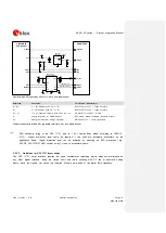
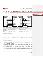
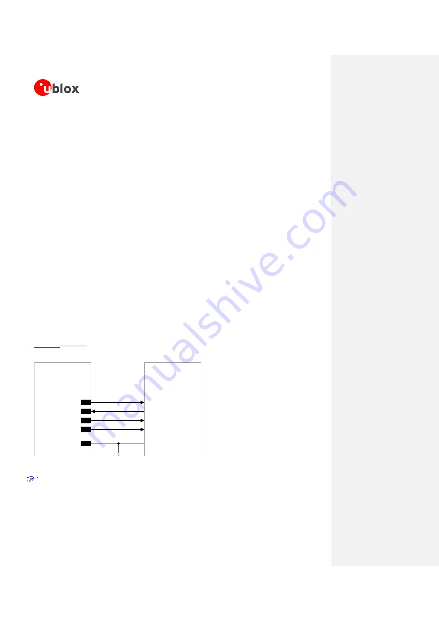
shows an application circuit with a generic digital audio device.
36
I2S_CLK
34
I2S_WA
I
2
S Clock
I
2
S Word Alignment
SARA-G350
35
I2S_TXD
37
I2S_RXD
I
2
S Data Input
I
2
S Data Output
GND
GND
1.8 V Digital
Audio Device
Figure 60: I
2
S interface application circuit with a generic digital audio device
Any external signal connected to the digital audio interface must be tri-stated or set low when the
module is in power-down mode and during the module power-on sequence (at least until the
activation of the
V_INT
supply output of the module), to avoid latch-up of circuits and allow a
proper boot of the module. If the external signals connected to the wireless module cannot be tri-

