


your position is our focus
D Migration to ANTARIS
®
4 receivers
Migrating
ANTARIS
®
to
an
ANTARIS
®
4
GPS
receiver
is
a
very
straightforward
procedure.
Nevertheless
there
are
during
the
migration.
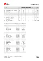
D.1 Software Changes
some
points
to
be
considered
< Firmware 5.00 or
< ROM5
Firmware 5.00 or
ROM5
Remarks
UBX-CFG-NAV
UBX-CFG-NAV2
To
ease
the
navigation
configuration
u-blox
has
introduced
a
new
message.
It
has
also
additional
features.
UBX-CFG-NAV
is
not
supported
anymore
on
ANTARIS
®
4.
See
also
Section 4.6
.
UBX-TIM-TM
UBX-CFG-TM
N/A
Time
mark
feature
Starting
with
firmware
version
5.0,
these
messages
are
not
longer
supported!
N/A
UBX-TIM-TM2
UBX-CFG-TM2
Improved
Time
Mark
feature.
Only
supported
on
LEA-4T.
UBX-RXM-RAW
UBX-RXM-SFRB
UBX-RXM-RAW
UBX-RXM-SFRB
Satellite
RAW
and
subframe
data.
These
messages
have
the
same
format
as
on
ANTARIS
®
but
on
ANTARIS
®
4
receivers
they
are
only
supported
on
LEA-4T
receivers.
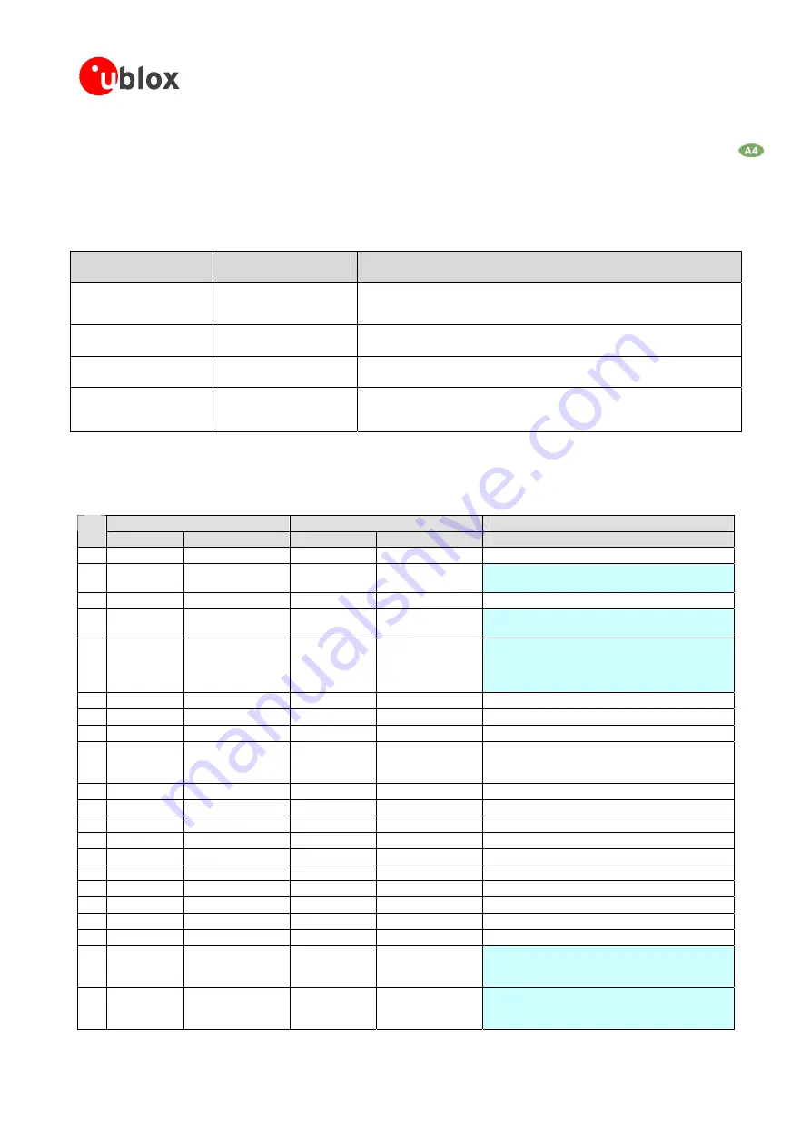
D.2 Migration from LEA-LA to LEA-4A/LEA-4S
The
pin-outs
of
LEA-LA
and
LEA-4A/LEA-4S
modules
do
not
differ
significantly.
Table 79
compares
the
modules
and
highlights
the
differences
to
be
considered.
LEA-LA
LEA-4A / LEA -4S
Remarks for Migration
Pin
Pin
Name
Typical
Assignment
Pin
Name
Typical
Assignment
1 TXD2
VDDIO
level
I/O
TXD2
VDDIO
level
I/O
No
difference.
2 RXD2
VDDIO
level
I/O;
pull
up
if
not
used
RXD2
VDDIO
level
I/O;
not
connected
Do
not
add
an
external
pull
up
resistor;
there
is
one
built-in
to
V_BAT
.
Leave
open
if
not
used.
3 TXD1
VDDIO
level
I/O
TXD1
VDDIO
level
I/O
No
difference
4 RXD1
VDDIO
level
I/O;
pull
up
if
not
used
RXD1
VDDIO
level
I/O
Do
not
add
an
external
pull
up
resistor;
there
is
one
built-in
to
V_BAT
.
Leave
open
if
not
used.
5 VDDIO
1.65
–
3.60V
VDDIO
1.65
–
3.60V
To
be
compatible
to
LEA-LA,
VDDIO
has
to
be
set
to
Vcc
to
assure
a
3.0V
level
at
the
serial
ports.
The
GPSMODE
pins
do
recognize
1.8V
and
3.0V
as
“high”
value
at
VDDIO
.
6 VCC
2.70
–
3.30V
VCC
2.70
–
3.30V
No
difference
7 GND
GND
GND
GND
No
difference
8 VDD18OUT
Not
connected
VDD18OUT
Not
connected
No
difference
9 GPSMODE6
Connected
to
GND
or
VDD_18OUT
GPSMODE6
Not
connected
Backward
compatible:
This
pin
can
be
connected
to
GND,
VDD18OUT
or
VCC.
An
external
pull
up
resistor
is
not
required
as
there
is
one
built-in.
10 RESET_N
1.8V
RESET_N
1.8V
No
difference
(see
Section
4.9.2
).
11 V_BAT
1.95
–
3.6V
V_BAT
1.50
–
3.6V
Wider
voltage
range.
Uncritical
for
migration.
12 BOOT_INT
NC
BOOT_INT
N
No
difference
C
13 GND
GND
GND
GND
No
difference
14 GND
GND
GND
GND
No
difference
15 GND
GND
GND
GND
No
difference
16 RF_IN
RF_IN
RF_IN
RF_IN
No
difference
17 G
fference
ND
GND
GND
GND
No
di
18 VCC_RF
VCC
-
0.1V
VCC_RF
VCC
-
0.1V
No
difference
19 V_ANT
3.0V
–5.0V
V_ANT
3.0V
-5.0V
No
difference
20 AADET_N
Connected
to
GND
AADET_N
Not
connected
No
external
pull
down
resistor
required,
as
there
is
already
an
internal
pull
down
resistor.
Please
check
resistor
values
in Section 4.3.3.2
21 GPSMODE5
Connected
to
GND
or
VDD_18OUT
GPSMODE5
Not
connected
Backward
compatible:
This
pin
can
be
connected
to
GND,
VDD18OUT
or
VCC.
An
external
pull
up
resistor
is
not
required
as
there
is
one
built-in.
GPS
Modules
-
System
Integration
Manual
(SIM)
(incl.
Reference
Design)
Migration
to
ANTARISP®P4
receivers
GPS.G4-MS4-05007-A1
Page 167


