User's Manual l MBa8Xx UM 0100 l © 2020, TQ-Systems GmbH
Page 41
3.8.14
JTAG
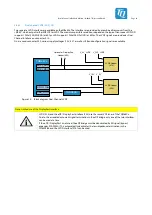
The JTAG interface is routed to a 20-pin header (X15). The required pull-ups of the lines TDI, TMS, and SRST# are available on the
MBa8Xx. All signal lines use 1.8 V as reference voltage. The JTAG interface is not ESD protected.
The JTAG mode can be configured by a placement option. Information on this can be found in the MBa8Xx schematics.
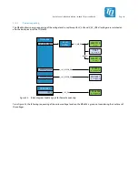
TQMa8Xx
JTAG_TCK
JTAG_TDI
JTAG_TDO
JTAG_TMS
20-pin
Header
(X15)
Figure 20: Block diagram JTAG
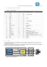
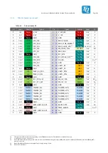
Table 44:
Pinout JTAG (X15)
Pin
Signal
Dir.
Level
Remark
1
JTAG_VREF
P
1.8 V
1.8 V reference voltage for debugger (via series resistor 100 Ω at V_1V8)
2
V_1V8
P
1.8 V
(31)
1.8 V supply voltage for debugger
3
SCU_WDOG_OUT O
PU
1.8 V
Watchdog output of i.MX 8
4
GND
P
0 V
Ground
5
JTAG_TDI
I
PU
1.8 V
Test Data In
6
GND
P
0 V
Ground
7
JTAG_TMS
I
PU
1.8 V
Test Mode Select
8
GND
P
0 V
Ground
9
JTAG_TCK
I
PD
1.8 V
Test Clock
10
GND
P
0 V
Ground
11
NC
I
PD
1.8 V
Not used (pulled to GND)
12
GND
P
0 V
Ground
13
JTAG_TDO
O
1.8 V
Test Data Out
14
GND
P
0 V
Ground
15
JTAG_SRST#
I/O
PU
1.8 V
System Reset (see also chapter 3.11)
16
GND
P
0 V
Ground
17
NC
I
PU
1.8 V
Not used (pulled to V_1V8)
18
GND
P
0 V
Ground
19
NC
I
PD
1.8 V
Not used (pulled to GND)
20
GND
P
0 V
Ground
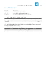
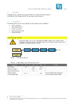
By default the debugger is supplied with 1.8 V at X15-2. Alternatively, the supply voltage can be changed to 3.3 V using the
placement option. The maximum output current is 10 mA. The following table shows the corresponding changes.
Table 45:
Assembly option Supply voltage JTAG
Voltage
R141
R142
Remark
1.8 V (V_1V8)
0 Ω
NP
Default
3.3 V (V_3V3_MB)
NP
0 Ω
–
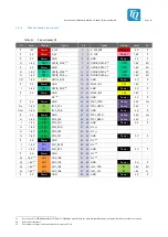
31:
Can be changed by assembly option, see Table 45.


