


User's Manual l TQMa8XxS UM 0101 l © 2022, TQ-Systems GmbH
Page 26
3.3.14
Boot Select
The Boot Select signals and FORCE_RECOV# are logically linked by a CPLD and converted into the corresponding BOOT_MODE
signals for the i.MX 8X. For further details see section 3.2.1.3.
3.3.15
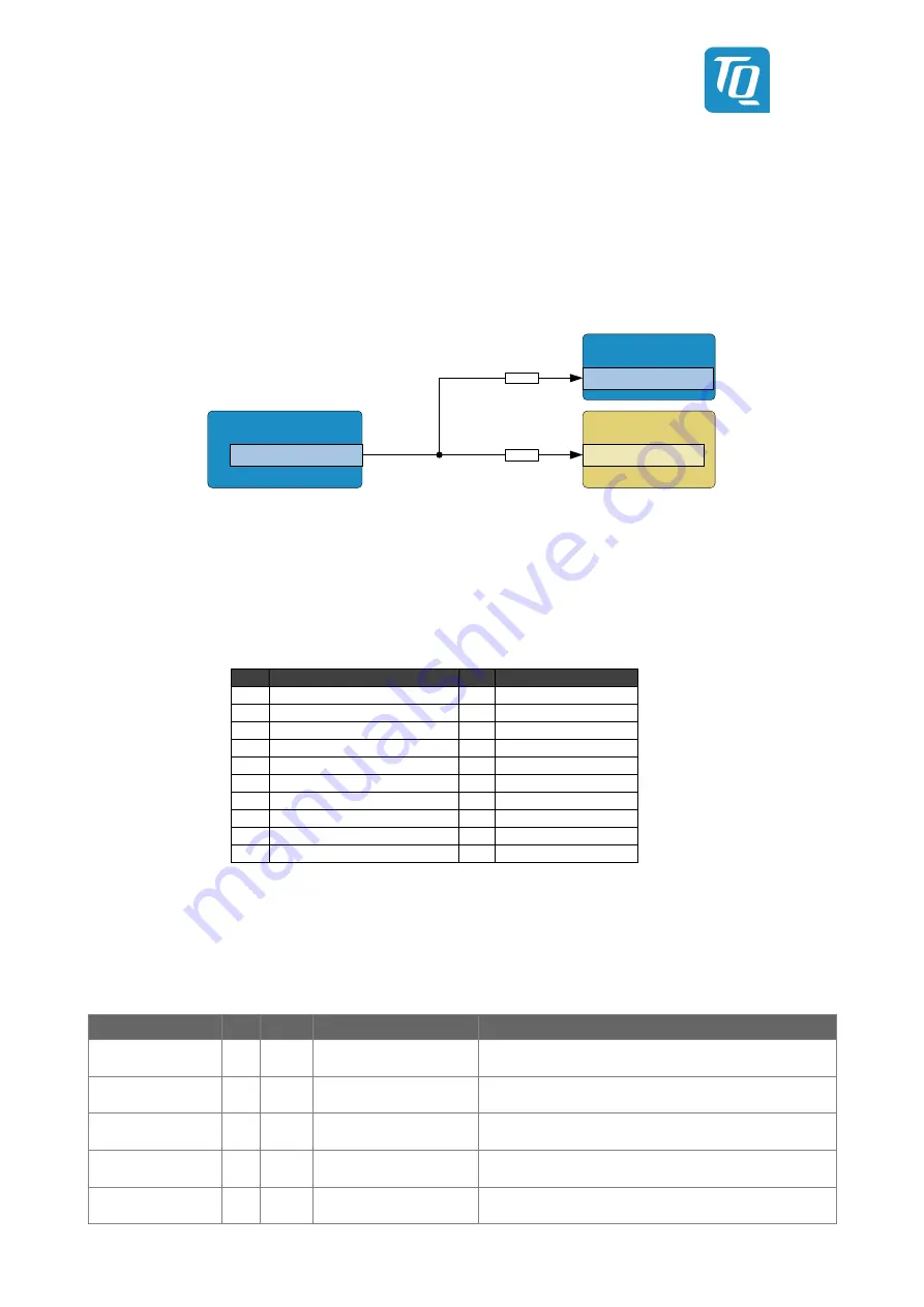
Watchdog
The watchdog signal SCU_WDOG0_WDOG_OUT of the i.MX 8X is connected to the watchdog input of the PMIC and to the
SMARC pin WDT_TIME_OUT#. Both can be disconnected via 0R jumper.
i.MX 8X
SMARC-Pins
WDT_TIME_OUT#
SCU_WDOG_OUT
PF8100
WDI
Figure 23: Block diagram Watchdog
3.3.16
JTAG
The JTAG interface of the i.MX 8X is provided on an optional connector X2 on the TQMa8XxS. In addition, test points are
provided at the JTAG signals. The optional connector and the pin assignment are defined in the SMARC specification (6).
Table 16: Pin assignment JTAG connector
Pin
Name (SMARC spec.)
I/O Signal (CPU ball)
1
VDD_JTAG_IO
P
V_1V8
2
JTAG_TRST#
-
NC
3
JTAG_TMS
I
JTAG_TMS (AG35)
4
JTAG_TDO
O
JTAG_TDO (AF32)
5
JTAG_TDI
I
JTAG_TDI (AH34)
6
JTAG_TCK
I
JTAG_TCK (AE31)
7
JTAG_RTCK
I
NC
8
GND
P
GND
9
MFG_MODE#
I
NC
10
GND
P
GND
3.4
Management pins
The SMARC standard provides a large number of control signals, which can be roughly divided into two categories. The following
table shows an overview of the SMARC pins that are connected to the CPU (6):
Table 17:
Management pins
Signal
I/O
Level
Description
Usage
CARRIER_STBY#
O
1.8 V
Standby status
SCU_PMIC_STANDBY from i.MX 8X to PMIC (low-active),
linked to CARRIER_PWR_ON (see Figure 24)
POWER_BTN#
I
1.8 V
i.MX 8X ON/OFF
i.MX 8X ON_OFF_BUTTON
SLEEP#
I
1.8 V
Carrier Sleep Status
i.MX 8X GPIO0_IO13
(Debouncing via RC element and Schmitt Trigger)
LID#
I
1.8 V
Enclosure status
i.MX 8X GPIO0_IO12
(Debouncing via RC element and Schmitt Trigger)
BATLOW#
I
1.8 V
Low battery voltage
i.MX 8X GPIO0_IO16


