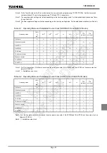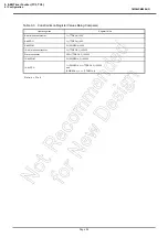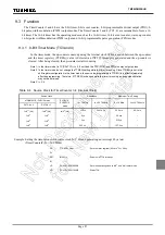
Page 97
TMP86PM29BUG
9.3.8
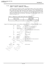
16-Bit Programmable Pulse Generate (PPG) Output Mode (TC3 and 4)
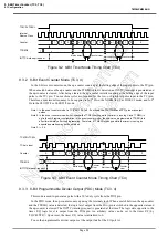
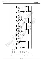
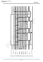
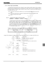
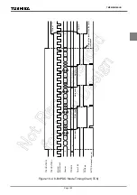
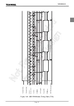
This mode is used to generate pulses with up to 16-bits of resolution. The timer counter 3 and 4 are cascad-
able to enter the 16-bit PPG mode.
The counter counts up using the internal clock or external clock. When a match between the up-counter and
the timer register (PWREG3, PWREG4) value is detected, the logic level output from the timer F/F4 is
switched to the opposite state. The counter continues counting. The logic level output from the timer F/F4 is
switched to the opposite state again when a match between the up-counter and the timer register (TTREG3,
TTREG4) value is detected, and the counter is cleared. The INTTC4 interrupt is generated at this time.
Since the initial value can be set to the timer F/F4 by TC4CR<TFF4>, positive and negative pulses can be
generated. Upon reset, the timer F/F4 is cleared to 0.
(The logic level output from the
PPG
4 pin is the opposite to the timer F/F4.)
Set the lower byte and upper byte in this order to program the timer register. (TTREG3
→
TTREG4,
PWREG3
→
PWREG4) (Programming only the upper or lower byte should not be attempted.)
For PPG output, set the output latch of the I/O port to 1.
Note 1: In the PPG mode, do not change the PWREGi and TTREGi settings while the timer is running. Since
PWREGi and TTREGi are not in the shift register configuration in the PPG mode, the new values pro-
grammed in PWREGi and TTREGi are in effect immediately after programming PWREGi and TTREGi.
Therefore, if PWREGi and TTREGi are changed while the timer is running, an expected operation may not
be obtained.
Note 2: When the timer is stopped during PPG output, the
PPG
4 pin holds the output status when the timer is
stopped. To change the output status, program TC4CR<TFF4> after the timer is stopped. Do not change
TC4CR<TFF4> upon stopping of the timer.
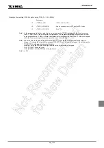
Example: Fixing the
PPG
4 pin to the high level when the TimerCounter is stopped
CLR (TC4CR).3: Stops the timer
CLR (TC4CR).7: Sets the
PPG
4 pin to the high level
Note 3: i = 3, 4
Two machine cycles are required for the high- or low-level pulse input to the TC3 pin. Therefore, a maxi-
mum frequency to be supplied is fc/2
4
Hz in the NORMAL1/2 or IDLE1/2 mode, and fs/2
4
to in the SLOW1/
2 or SLEEP1/2 mode.
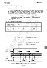
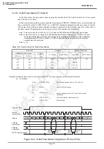
Example :Generating a pulse with 1-ms high-level width and a period of 16.385 ms (fc = 16.0 MHz)
Setting ports
LDW
(PWREG3), 07D0H
: Sets the pulse width.
LDW
(TTREG3), 8002H
: Sets the cycle period.
LD
(TC3CR), 33H
: Sets the operating clock to fc/2
3
, and16-bit PPG mode
(lower byte).
LD
(TC4CR), 057H
: Sets TFF4 to the initial value 0, and 16-bit
PPG mode (upper byte).
LD
(TC4CR), 05FH
: Starts the timer.
Summary of Contents for TLCS-870/C Series
Page 1: ...8 Bit Microcontroller TLCS 870 C Series TMP86PM29BUG ...
Page 6: ...TMP86PM29BUG ...
Page 7: ...Revision History Date Revision 2007 10 11 1 First Release 2008 8 29 2 Contents Revised ...
Page 9: ......
Page 15: ...vi ...
Page 19: ...Page 4 1 3 Block Diagram TMP86PM29BUG 1 3 Block Diagram Figure 1 2 Block Diagram ...
Page 23: ...Page 8 1 4 Pin Names and Functions TMP86PM29BUG ...
Page 48: ...Page 33 TMP86PM29BUG ...
Page 49: ...Page 34 2 Operational Description 2 3 Reset Circuit TMP86PM29BUG ...
Page 61: ...Page 46 3 Interrupt Control Circuit 3 8 External Interrupts TMP86PM29BUG ...
Page 81: ...Page 66 6 Watchdog Timer WDT 6 3 Address Trap TMP86PM29BUG ...
Page 135: ...Page 120 10 8 Bit TimerCounter TC5 TC6 10 1 Configuration TMP86PM29BUG ...
Page 145: ...Page 130 11 Asynchronous Serial interface UART 11 9 Status Flag TMP86PM29BUG ...
Page 165: ...Page 150 13 10 bit AD Converter ADC 13 6 Precautions about AD Converter TMP86PM29BUG ...
Page 183: ...Page 168 15 LCD Driver 15 4 Control Method of LCD Driver TMP86PM29BUG ...
Page 201: ...Page 186 18 Electrical Characteristics 18 9 Handling Precaution TMP86PM29BUG ...
Page 203: ...Page 188 19 Package Dimensions TMP86PM29BUG ...
Page 205: ......


