background image

DISASSEMBLY INSTRUCTIONS

B3-2

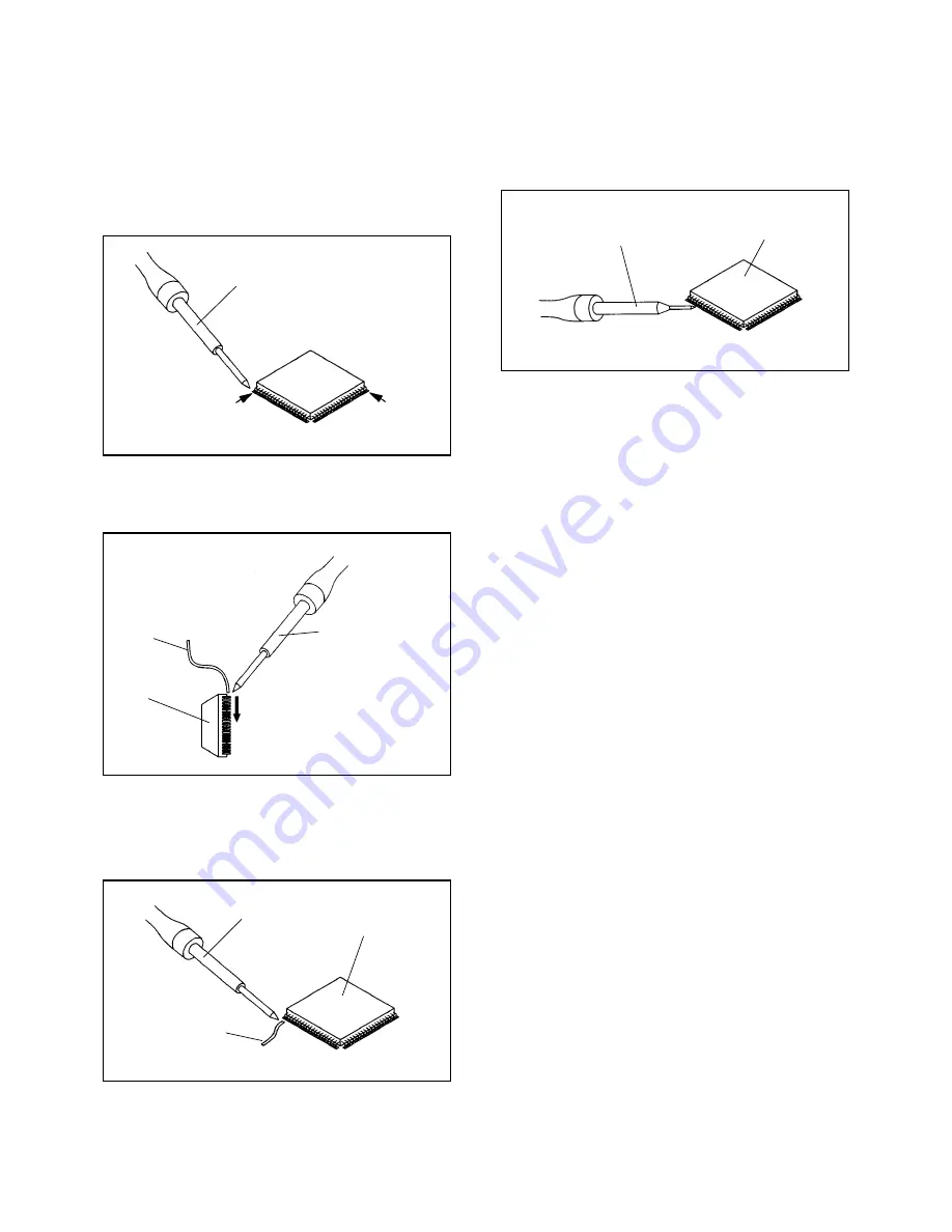
Supply soldering
from upper position
to lower position

IC

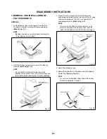
Supply the solder from the upper position of IC leads
sliding to the lower position of the IC leads.
 (Refer to Fig. 3-6.)

2.

Fig. 3-6

Soldering Iron

Solder

IC

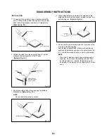
Absorb the solder left on the lead using the Braided
Shield Wire. (Refer to Fig. 3-7.)

3.

Fig. 3-7

Soldering Iron

Braided Shield Wire

NOTE

Do not absorb the solder to excess.

IC

When bridge-soldering between terminals and/or the
soldering amount are not enough, resolder using a Thin-
tip Soldering Iron. (Refer to Fig. 3-8.)

4.

Fig. 3-8

Thin-tip Soldering Iron

NOTE

When the IC leads are bent during soldering and/or
repairing, do not repair the bending of leads. If the
bending of leads are repaired, the pattern may be
damaged. So, be always sure to replace the IC in this
case.

Finally, confirm the soldering status on four sides of the
IC using a magnifying glass.
Confirm that no abnormality is found on the soldering
position and installation position of the parts around the
IC. If some abnormality is found, correct by resoldering.

5.

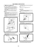
Solder temporarily

Soldering Iron

INSTALLATION

Take care of the polarity of new IC and then install the
new IC fitting on the printed circuit pattern. Then solder
each lead on the diagonal positions of IC temporarily.
(Refer to Fig. 3-5.)

1.

Fig. 3-5

Solder temporarily

Summary of Contents for MD20FM3

Page 1: ...SERVICE MANUAL COLOR TELEVISION DVD VIDEO PLAYER FILE NO 140 200221 MD20FM3 ...

Page 2: ...OLS ADJUSTMENTS OR THE PERFORMANCE OF PROCEDURES OTHER THAN THOSE SPECIFIED HEREIN MAY RESULT IN HAZARDOUS RADIATION EXPOSURE TO PREVENT DIRECT EXPOSURE TO LASER BEAM DO NOT TRY TO OPEN THE ENCLOSURE VISIBLE LASER RADIATION MAY BE PRESENT WHEN THE ENCLOSURE IS OPENED DO NOT STARE INTO BEAM Location of the required Marking The rating sheet and the safety caution are on the rear of the unit CERTIFIC...

Page 3: ...ether there are the portions which are deteriorated around the serviced places serviced or not Check the insulation between the antenna terminal or external metal and the AC cord plug blades And be sure the safety of that INSULATION CHECK PROCEDURE 1 2 3 4 Unplug the plug from the AC outlet Remove the antenna terminal on TV and turn on the TV Insulation resistance between the cord plug terminals a...

Page 4: ...nto the outlet try reversing the plug If the plug should still fail to fit contact your electrician to replace your obsolete outlet Do not defeat the safety purpose of the polarized plug If your unit is equipped with a 3 wire grounding type plug a plug having a third grounding pin this plug will only fit into a grounding type power outlet This too is a safety feature If you are unable to insert th...

Page 5: ...eating and fire HEADPHONES When you use the headphones keep the volume at a moderate level If you use the headphones continuously with high volume sound it may cause hearing damage LEASER BEAM Do not look into the opening of the disc tray or ventilation opening of the product to see the source of the laser beam It may cause sight damage DISC Do not use a cracked deformed or repaired disc These dis...

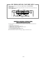
Page 6: ...ORD CANCELLATION If the stored 4 digit password in the Rating Level menu needs to be cancelled please follow the steps below Turn Unit ON Confirm that no disc on the disc tray Press and hold the 7 key on the remote control unit Simultaneously press and hold the STOP key on the front panel Hold both keys for more than 3 seconds The On Screen Display message Initialize will appear The 4 digit passwo...

Page 7: ... CONTROL RATING LEVEL TABLE OF CONTENTS GENERAL SPECIFICATIONS DISASSEMBLY INSTRUCTIONS 1 REMOVAL OF MECHANICAL PARTS AND P C BOARDS 2 REMOVAL OF ANODE CAP 3 REMOVAL AND INSTALLATION OF FLAT PACKAGE IC SERVICE MODE LIST CONFIRMATION OF HOURS USED WHEN REPLACING EEPROM MEMORY IC SERVICING FIXTURES AND TOOLS ELECTRICAL ADJUSTMENTS BLOCK DIAGRAMS TV DVD POWER PRINTED CIRCUIT BOARDS SYSCON AV OPEARTIO...

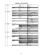
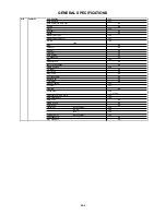
Page 8: ...em M System Tuner and System 1Tuner Receive CH Channel Tuner Others Tuning System F Synth Input Impedance VHF UHF 75 Ohm CH Coverage 2 69 4A A 5 A 1 A I J W W 1 W 84 Intermediate Picture FP 45 75MHz Frequency Sound FS 41 25MHz FP FS 4 50MHz Preset CH Stereo Dual TV Sound Yes NTSC Playback PAL60 No G 4 Power Power Source AC 120V 60Hz DC Power Consumption at AC 120W at 120V 60Hz at DC Stand by at AC...

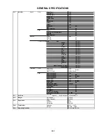
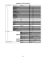
Page 9: ...apter Yes No A Yes No Music Calender 1 14 Play Yes No 7 seg Digit 9 Yes No Terminals Front Video Input Yes Audio Input Yes Stereo Other Terminal Head Phone Rear Video Input Rear1 Yes Video Input Rear2 No Audio Input Rear1 Yes Stereo Audio Input Rear2 No Video Output Yes Audio Output Yes Stereo Euro Scart No Digital Audio Output Coaxial Optical Audio Output No Color Stream No Diversity No Ext Speak...

Page 10: ...Code No Pin Code Registration No Pin Code No DVD RGB Composite No Game Yes Hotel Lock No Volume Yes Sound Mute No On Screen Menu DVD Yes Display Menu Type Character Rating Level Yes Audio Yes Sub Title Yes TV Screen Size Yes OSD Display On Off Yes Menu Language Yes Audio Output No Set Up Language Yes Password Lock Unlock Yes Open Yes Close Yes No disc Yes Reading Yes Play Yes Still Pause Yes Stop ...

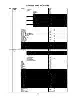
Page 11: ... No Play Yes Stop Yes Search Yes Search Yes Skip Yes Skip Yes Slow Yes Slow Yes Still Pause Yes Display Call Yes TV DVD Yes Clear Reset Yes Audio Audio Sel Yes Angle Yes Subtitle Yes Subtitle On Off No Title Yes Set up TV Menu TV MENU Yes Return Yes Menu DVD SET UP Yes Up Set CH Up Yes Down Set CH Down Yes Left Select Yes Right Select Yes Select Enter Yes Play Mode Yes Closed Caption Yes Input Yes...

Page 12: ...arch No CH Allocation No SAP Yes Channel Lock No Just Clock Function No Game Position Yes CH Label No VM Circuit No Area Code No FM Transmitter No Energy Star No TV Monitor No Closed Caption Yes Full OSD Yes Premiere No Comb Filter Yes 2 Lines Parental Lock DVD Only Yes Auto CH Memory Yes Hotel Lock No Stable Sound No Favorite CH No Digital Out Dolby Digital Yes PCM Yes DTS Yes Down Mix Out Dolby ...

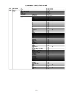
Page 13: ...75 Ohm Coaxial Cable No 21pin Cable No U V Mixer No Channel Film No Battery Yes UM size x pcs UM 4 x 2 pcs OEM Brand No DC Car Cord Center No AC Cord No AV Cord 2Pin 1Pin No AC Plug Adaptor No Safety Tip No Anntena Change Plug No 300 ohm to 75 ohm Antenna Adapter Yes G 17 Carton Master Carton No Content Sets Material Dimensions W x D x H mm Description of Origin Gift Box Yes Material Double White ...

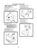
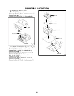
Page 14: ...ock 1 1 1 4 MAIN PCB Refer to Fig 1 4 1 2 3 4 Remove the 2 screws 1 Remove the 3 screws 2 Disconnect the following connectors CP810B CP820B and CP811 Remove the Main PCB in the direction of arrow Fig 1 4 1 1 Main PCB DVD Block 1 2 CRT PCB Refer to Fig 1 2 CAUTION BEFORE REMOVING THE ANODE CAP DISCHARGE ELECTRICITY BECAUSE IT CONTAINS HIGH VOLTAGE BEFORE ATTEMPTING TO REMOVE OR REPAIR ANY PCB UNPLU...

Page 15: ... SYSCON PCB CD DECK Refer to Fig 1 6 1 2 3 4 5 6 7 8 9 Remove the 3 screws 1 Remove the AV PCB in the direction of arrow A Remove the 4 screws 2 Remove the Angle Deck in the direction of arrow B Disconnect the following connectors CP4001 and CP4002 Remove the 4 screws 3 Remove the CD Deck in the direction of arrow C Remove the 4 screws 4 Remove the Syscon PCB in the direction of arrow D Fig 1 6 1 ...

Page 16: ...s the voltage is discharged Flip up the sides of the Rubber Cap in the direction of the arrow and remove one side of the support Refer to Fig 2 2 2 GND on the CRT Screwdriver Alligator Clip Support CRT GND on the CRT Rubber Cap CRT Support Fig 2 1 Fig 2 2 3 After one side is removed pull in the opposite direction to remove the other NOTE INSTALLATION 1 Clean the spot where the cap was located with...

Page 17: ...using a blower type IC desoldering machine Refer to Fig 3 2 2 Fig 3 2 NOTE Do not add the rotating and the back and forth directions force on the IC until IC can move back and forth easily after desoldering the IC leads completely When IC starts moving back and forth easily after desoldering completely pickup the corner of the IC using a tweezers and remove the IC by moving with the IC desoldering...

Page 18: ...3 8 Thin tip Soldering Iron NOTE When the IC leads are bent during soldering and or repairing do not repair the bending of leads If the bending of leads are repaired the pattern may be damaged So be always sure to replace the IC in this case Finally confirm the soldering status on four sides of the IC using a magnifying glass Confirm that no abnormality is found on the soldering position and insta...

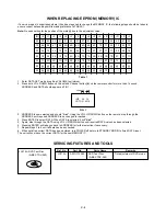
Page 19: ...ing and the POWER ON total hours 1 1 1 1 Initialization of the factory on DVD NOTE Do not use this for the normal servicing The function will only work without the setting of DVD disc at DVD mode While pressing the Remocon Key for more than the Standard Time press the Set Key simultaneously Releasing of PARENTAL LOCK Refer to the PARENTAL CONTROL RATING LEVEL NOTE The function will only work witho...

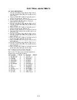
Page 20: ...5B 30 59 5B 7B 7B 5C 5C 7C 7C 5D 7D 7D 5E 5E 7E 7E 5F 40 5D 5F 5F 7F 7F 50 60 10 DVD Test Disc A BEX TDV 540 JG175A Ref No JG175A Part No APJG175A00 Parts Name DVD Test Disc A BEX TDV 540 Remarks Tint adjustment of DVD mode SERVICING FIXTURES AND TOOLS 3 4 5 6 7 8 The unit will now have the correct DATA for the new MEMORY IC ADDRESS is now selected and should blink Using the VOL UP DOWN button on ...

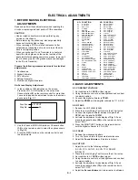
Page 21: ...gital voltmeter is 2 7 0 05V 1 Read and perform these adjustments when repairing the circuits or replacing electrical parts or PCB assemblies CAUTION Use an isolation transformer when performing any service on this chassis Before removing the anode cap discharge electricity because it contains high voltage When removing a PCB or related component after unfastening or changing a wire be sure to put...

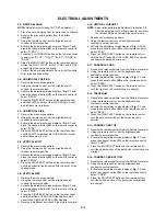
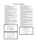
Page 22: ...ode display of Fig 1 1 and press the channel button 31 on the remote control to select CNRT Press the RIGHT LEFT button on the remote control until the upper section of the both ends vertical lines are straight 2 5 WHITE BALANCE NOTE Adjust after performing CUT OFF adjustment 1 2 3 4 5 6 7 Place the set with Aging Test for more than 15 minutes Receive the gray scale pattern from the Pattern Genera...

Page 23: ...minimum Set the multi sound signal generator L ch Non input R ch 1KHz and receive the RF signal Connect the oscilloscope to the Audio Out Jack L ch Then perform the above adjustments 3 7 Method 2 2 16 OSD HORIZONTAL Activate the adjustment mode display of Fig 1 1 and press the channel button 33 on the remote control to select OSD Press the RIGHT LEFT button on the remote control until the differen...

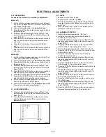
Page 24: ... CENTER Receive the color bar pattern RF Input Using the remote control set the brightness contrast color and tint to normal position Connect the oscilloscop to TP801 Activate the adjustment mode display of Fig 1 1 and press the channel button 09 on the remote control to select COLC Adjust the VOLTS RANGE VARIABLE knob of the oscilloscope until the range between white 100 and 0 is set to 4 scales ...

Page 25: ... 13 Activate the adjustment mode display of Fig 1 1 and press the channel button 15 on the remote control to select CNTX Press the RIGHT LEFT button on the remote control until the contrast step No becomes 61 Receive a broadcast and check if the picture is normal Press the INPUT SELECT button on the remote control to set to the AV mode Activate the adjustment mode display of Fig 1 1 and press the ...

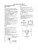
Page 26: ...s between the deflection yoke and CRT funnel to fix the deflection yoke Refer to Fig 3 2 b R G B R G B Fig 3 2 a WEDGE WEDGE WEDGE WEDGE POSITION Fig 3 2 b R G B R G B Receive the crosshatch pattern from the color bar generator Combine red and blue of the 3 color crosshatch pattern on the center of the screen by adjusting the pair of 4 pole magnets Combine red blue magenta and green by adjusting t...

Page 27: ... CP8002 CP8003 CRT CD801 CRT PCB J801 TP801 TP803 C P 8 5 0 B CP807 CP803B CP801 AC IN CRT C P 5 0 2 L503 CP507 CP506 CP401 CRT FB401 TP401 R449 CP803A CP403 VR502 CP820B CP810B CP811 TOP SHIELD CD402 TOP SHIELD CD502 CP8001 CP8005 CP8006 CD403 TU001 J7001 J7003 J7002 CP101 AV PCB OPERATION PCB SYSCON PCB CD810 CD820 CD850 CD401 CD803 CD501 CD8001 CD8002 CD4001 CD4002 MAIN PCB C P 8 0 0 4 ...

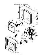
Page 28: ...W A 104 205 205 205 206 206 208 207 PCB070 MAIN PCB 128 207 109 206 205 206 109 208 I 1 201 201 201 201 201 201 121 119 207 203 203 203 203 124 118 118 PCB110 CRT PCB 101 116 103 120 PCB030 OPERATION PCB 204 B 204 204 204 204 ...

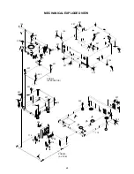
Page 29: ...ECHANICAL EXPLODED VIEW I 2 112 207 207 207 207 A 122 207 207 207 207 207 207 207 207 207 109 207 109 B 110 207 202 202 115 115 205 PCB250 AV PCB 206 207 207 207 207 126 207 207 207 207 PCB010 SYSCON PCB ...

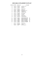
Page 30: ...823 CABINET BACK 122 BZ710406 702WSA0075 SHIELD TOP 124 BZ710258 741WUA0001 SPRING EARTH 126 BZ710407 712WPB0075 PLATE TRAY FRONT 128 BZ710260 899HV3T000 HOLDER ANODE WIRE 201 BZ710035 8117540A64 SCREW TAPPING B0 TRUSS 4x16 202 BZ710320 8117540804 SCREW TAPPING B0 TRUSS 4x8 203 BZ710275 8121J50B54 SCREW TAPPING B0 GW20 5x28 204 BZ710031 8110630A04 SCREW TAP TITE P BRAZIER 3x10 205 BZ710239 8109I30...

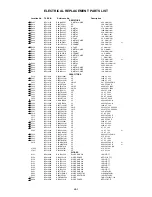
Page 31: ...E 10 UF 250V C433 BZ110020 E5EZT8220M CE 22 UF 100V C442 BZ110057 E53FF56R8K CE 6 8 UF 50V NP C450 BZ110182 C03L0R713K CC 0 001 UF 2KV R C502 BZ110009 C13HB07H3K CC 0 0022UF 2KV B C503 BZ110009 C13HB07H3K CC 0 0022UF 2KV B C504 BZ110039 E02LT1102M CE 1000 UF 10V C505 BZ110138 P2472B224M CMP 0 22UF 275V PHE840 C506 BZ110138 P2472B224M CMP 0 22UF 275V PHE840 C507 BZ110062 E51SFC821M CE 820 UF 200V C...

Page 32: ... BZ410022 D97U06R81B DIODE ZENER MTZJ6 8B T 77 D612 BZ410059 D2WT11ES10 DIODE SILICON 11ES1 EIC D613 BZ410006 D1VT001330 DIODE SILICON 1SS133T 77 D614 BZ410006 D1VT001330 DIODE SILICON 1SS133T 77 D615 BZ410006 D1VT001330 DIODE SILICON 1SS133T 77 D792 BZ410087 0021E2Q140 LED LTL 1CHEE 002A D805 BZ410006 D1VT001330 DIODE SILICON 1SS133T 77 D806 BZ410006 D1VT001330 DIODE SILICON 1SS133T 77 D807 BZ410...

Page 33: ...COMPOUND TRANSISTOR KRC111MAT Q501 BZ510077 TAAT012714 TRANSISTOR SILICON KTA1271_Y AT Q502 BZ510069 TCATC31980 TRANSISTOR SILICON KTC3198 AT Y GR Q503 BZ510015 TCWQ4160E0 TRANSISTOR SILICON 2SC4160 OEC YAC1 Q504 BZ510069 TCATC31980 TRANSISTOR SILICON KTC3198 AT Y GR Q505 BZ410088 0002E00610 PHOTO COUPLER LTV 817M VB Q507 BZ510069 TCATC31980 TRANSISTOR SILICON KTC3198 AT Y GR Q508 BZ510032 TD3T012...

Page 34: ...6 BZ310124 02AHA896A1 CORE FERRITE W5T18 4X10X9 6 L758 BZ310041 02167F101J COIL 100 UH L801 BZ310118 02AHB9A972 CORE FERRITE W5T29X7 5X19 L802 BZ310069 02167D151K COIL 150 UH L803 BZ310069 02167D151K COIL 150 UH L804 BZ310069 02167D151K COIL 150 UH L810 BZ310118 02AHB9A972 CORE FERRITE W5T29X7 5X19 or BZ310132 02AXB9A971 CORE FERRITE ESD R 30SD L811 BZ310118 02AHB9A972 CORE FERRITE W5T29X7 5X19 L9...

Page 35: ...BZ613030 1022045R72 FILTER SAW SAFGP45M7VFYZR0B CF204 BZ613018 1012T04702 FILTER CERAMIC TRAP MKT47 3MC110P TF CP101 BZ614238 0697260650 CONNECTOR PCB SIDE TKC M06X A1 CP102 BZ614239 069S290639 CONNECTOR PCB SIDE A2001WR2 9P CP303 BZ614214 069S2B0629 CONNECTOR PCB SIDE A2001WV2 11P CP401 BZ614240 069X460029 CONNECTOR PCB SIDE B06B DVS CP403 BZ614444 069D01001A CONNECTOR PCB SIDE 003P 2100 or BZ614...

Page 36: ...AKER SG04H02BRA or BZ614253 070W546003 SPEAKER MSF 18D5SB05 02 SP352 BZ614381 070C546004 SPEAKER SG04H02BRA or BZ614253 070W546003 SPEAKER MSF 18D5SB05 02 TH501 BZ410079 DF5EL3R0A0 DEGAUSS ELEMENT ZPB45BL3R0A TM101 BZ614429 076D0EF010 TRANSMITTER TOT201N09080 TU001 BZ610125 0145K00055 TUNER VHF UHF TECC1040PG32D V801 BZ614453 098W210433 CRT W DY A51LVV196X10 O X101 BZ613019 1002T01606 CERAMIC OSCI...

Page 37: ...OLS ADJUSTMENTS OR THE PERFORMANCE OF PROCEDURES OTHER THAN THOSE SPECIFIED HEREIN MAY RESULT IN HAZARDOUS RADIATION EXPOSURE TO PREVENT DIRECT EXPOSURE TO LASER BEAM DO NOT TRY TO OPEN THE ENCLOSURE VISIBLE LASER RADIATION MAY BE PRESENT WHEN THE ENCLOSURE IS OPENED DO NOT STARE INTO BEAM Location of the required Marking The rating sheet and the safety caution are on the rear of the unit CERTIFIC...

Page 38: ...RESET IC102 PST600C AT 5 6V Q204 BUFFER Q202 Q203 BUFFER STOP SKIP FF OPEN CLOSE PLAY VOL UP CH DOWN VOL DOWN CH UP FROM OPERATION BLOCK 32 31 X101 16MHz TV BLOCK DIAGRAM 5 38 4 37 AV SW IC701 MM1311AD 24 15 8 13 10 23 17 18 B 2 31 30 32 4 7 1 14 Q753 BUFFER 25 Q702 BUFFER SOUND DECORDER IC902 AN5829S 14 19 18 22 21 R V J7003 6 2 4 L J7002 Q7016 BUFFER Q7006 BUFFER AUDIO SW IC7002 CD4053BNSR 12 5 ...

Page 39: ...C CLK27 YUVO 7 C B ZERO L R CVBS Y C ANALOGUE AUDIO OUT ANALOGUE YC OUT AUDIO SW IC8504 SN74LV4052APW SPDIF DVD SPDIF CD Q7001 Q7002 LINE DRIVER B A J7001 COAXIAL DIGITAL AUDIO X1001 12 5MHz B CTRL BUS FROM_SYSCON DVD L CD H DVD CD HD0 7 SYSCON IC1001 ZR36703 SSC FROM_SYSCON SCLK TO_SYSCON ATN HRST TO TV BLOCK RESET RESET TX RX DVD RESET SYS MUTE SCL SDA SCL SDA SCL SDA A P CON 3 3V B P CON D5V C ...

Page 40: ...IVE SW Q508 5 6V REG Q150 P CON 5V DRIVER Q153 3 1 5V REG IC154 KIA7805API 3 1 5V REG IC503 KIA7805API P CON 12V DRIVER Q157 P CON 3 3V OUT Q158 Q159 Q160 3 1 5V REG IC152 KIA7805API 3 1 9V REG IC153 KIA7809API F502 P CON SW Q152 P CON 3 3V OUT Q154 Q155 Q156 POWER BLOCK DIAGRAM DEGAUSS_H P CON 3 3V P CON D5V P CON 3 3V_A AT 5 6V AT 8V SOUND B AT 8V AT 6V FBT 12V P CON 9V P CON 9V P CON 5V D B TV ...

Page 41: ...506 D8507 D8508 IC1001 IC1006 IC4001 IC4002 IC4004 IC8501 IC8503 IC8504 L8501 L8503 L8504 Q8501 R1001 R1002 R1003 R1004 R1005 R1006 R1007 R1008 R1009 R1010 R1011 R1012 R1014 R1015 R1016 R1017 R1018 R1019 R1023 R1024 R1027 R1028 R4001 R4002 R4003 R4004 R4005 R4006 R4007 R4008 R4009 R4010 R4011 R4012 R4013 R4014 R4015 R4016 R4017 R4018 R4020 R4021 R4024 R4025 R4027 R4028 R4029 R8501 R8502 R8503 R850...

Page 42: ...4 IC152 IC153 CP8004 W068 W067 R8026 W008 R7052 C907 C7040 W103 W006 W007 W063 IC701 W106 W096 W095 W022 W824 W834 C718 C717 W143 W077 R701 W144 W145 W146 C715 C716 W148 C701 W164 C706 C705 C704 W026 W163 W029 W030 W027 W104 CP101 D613 D614 D615 W178 R215 R216 L001 W845 X101 W217 C155 C160 C153 W186 W155 W156 R709 R708 C7042 C7043 W228 W229 L7004 W213 W185 W843 J7003 W130 W083 W055 W059 CP8003 CP8...

Page 43: ...624 R617 C622 R607 R608 R609 R612 R613 C612 R614 R629 R631 R628 R627 R605 C605 C203 C218 C220 C606 C222 C214 C201 R217 C208 R218 R219 R214 Q205 C202 R213 C632 R623 R165 R172 Q155 Q156 R151 Q159 Q160 R152 Q152 R313 R317 R324 R325 C324 C321 C322 C304 IC301 C326 C315 C317 R314 R306 R303 R310 R312 C311 C314 R309 C316 C318 R315 R304 R301 R184 R154 C348 C307 Q301 R302 C7024 C7015 R7021 R7016 R7010 Q7001...

Page 44: ...R775A R776 R777 R778 SW791 SW792 SW793 SW794 SW795 SW796 SW797 SW798 SW799 W804 W806 W809 W002 W007 W008 W010 W013 W014 C755A W015 W016 W017 W019 W020 CD355 CD356 W005 CD757_1 W004 W023 W009 W012 W024 W011 OS753 SW751_1 W813 W812 W808 C352_1 W018 PRINTED CIRCUIT BOARDS OPERATION SOLDER SIDE F 7 F 8 ...

Page 45: ... Q804_1 R810_1 TP801 C809 R814 Q806_1 R801 CP807 CP803B C535 W050 W051 R807 C501 W002 C527 W004 C523 C504 W001 W831 W029 W005 HS402 D402 W049 L802 L803 L804 Q807 D805 R817 Q808 D807 R804 Q809 R818 D806 CP810B W009 HS502_1 Q511 R508 D536 R524 W016 W028 CD402 C528 D533 D511 D534 W010 C517_2 C514_3 C450_2 C 4 2 4 _ 3 D527 D519 R509 Q501 W012 C531 C431 CP850B W053 C405 C404 C403 C524 C537 C433 C418 S5...

Page 46: ...4 YUV2 HA3 YUV3 HA2 YUV4 HRST HA1 YUV5 SSC MRST SSC MTSR HWR YUV6 SSC SCLK SSC ATN HD7 HD6 MPGCS YUV7 HD5 HD4 HRD HD3 MA4 HD2 HSYNC MA3 HD1 MA5 HD0 VSYNC MA2 HA4 MA6 HA3 MA1 HA2 MA7 HA1 MPGIRQ MA0 HWR MA8 MPGCS MA10 HRD MA9 MPGIRQ MA11 MPGRST MCS0 MPGSTBY MRAS HRDY MPCLK MCAS MWE MDQM MD8 MD7 MD9 MD6 MD10 MD5 MD11 MD4 MD12 MD3 MD13 MD2 MD14 MD1 MD15 MD0 MA4 MA3 MA5 MA2 MA6 MA1 MA7 MA0 MA8 MA10 MA9...

Page 47: ... MA11 MCS0 MRAS MPCLK MCAS MD13 MD2 MWE MDQM MD8 MD12 MD3 MD7 MD9 MD6 MD10 MD5 MD11 MD11 MD4 MD4 MD12 MD3 MD10 MD5 MD13 MD2 MD14 MD1 MD15 MD0 MD9 MD6 MD8 MD7 MDQM MDQM MWE MPCLK MCAS MRAS MCS0 MA9 MA11 MA8 MA10 MA7 MA0 MA6 MA1 MA5 MA2 MA4 MA3 P CON 3 3V SD DGND FROM TO MPEG SYSCON PCB SDRAM SCHEMATIC DIAGRAM FROM VIDEO ENCORDER PCB010 VMA215 3 3 NC NC VSS I O15 I O14 VSSQ I O13 I O12 VCCQ I O11 I ...

Page 48: ...CS HRD MPGIRQ MPGRST HD6 MPGSTBY HRDY HD5 HD4 HD3 HD2 HD1 HD0 MPGIRQ MPGRST MPGSTBY DVD_RESET MIC_ON RESET MPGCS CD DVD HRD HWR SW1 VD FROM TO VIDEO ENCORDER FROM TO MPEG NC NC NC NC 3 2 0 0 NC NC NC NC NC NC NC NC NC VCC P47 A07 P46 A06 P45 A05 P44 A04 P43 A03 P42 A02 P41 A01 VCC P40 A00 P37 D31 VSS P36 D30 P35 D29 P34 D28 P33 D27 P32 D26 P31 D25 P30 D24 P27 D23 P26 D22 P25 D21 P24 D20 P23 D19 P2...

Page 49: ...AGRAM IS THE LATEST AT THE TIME DIGITAL AUDIO SIGNAL PB AUDIO SIGNAL PB PLAYBACK COLOR SIGNAL PLAYBACK LUMINANCE SIGNAL P CON 3 3VA DGND P CON 3 3V MP P CON 3 3V AMCLK CLK27 SI2 ABCLK ALRCLK SO2 SPDIF DVD SSC MRST ASDAT0 YUV0 YUV0 SSC MTSR YUV1 SW1 YUV2 YUV1 YUV3 DVD_RESET YUV4 YUV2 D_LOAD H YUV5 YUV6 YUV7 YUV3 HSYNC VSYNC YUV4 SPDIF CD DM1 AIN YUV5 D_LOAD H YUV6 YUV7 DGND SPDIF P CON 3 3V SD DVD_...

Page 50: ...TS MARKED BY CAUTION DIGITAL AUDIO SIGNAL PB PLAYBACK VIDEO SIGNAL AUDIO SIGNAL PB CAUTION DIGITAL TRANSISTOR PLAYBACK COLOR SIGNAL PLAYBACK LUMINANCE SIGNAL CP8004 51048 1110 1 10 11 2 3 4 5 6 7 8 9 CP8005 51048 1210 1 10 11 12 2 3 4 5 6 7 8 9 L151 W5T29X7 5X19 CD8002 2S0I0101 CD8001 2S0I0101 R168 2 7K 1 R170 10K 1 R182 2 7K 1 R169 10K 1 R171 10K 1 R183 10K 1 SOUND_GND SOUND B P CON 9V P CON A5V ...

Page 51: ...ME DANS LA NOMENCLATURE DES PIECES N UTILISER QUE CELLS DECRITES DANGEREUSES AN POINT DE VUE SECURITE ETANT LES PIECES REPAREES PAR UN ATTENTION DESCRIBED IN PARTS LIST ONLY CRITICAL FOR SAFETY USE ONES ARE SINCE THESE PARTS MARKED BY CAUTION PLAYBACK VIDEO SIGNAL SCL SDA I2C_OFF TUNER_AGC TV DVD TUNER_IF P CON 30V TUNER_AGC EXT_MUTE CHROMA 5V SDA SCL SWD_V OUT TUNER_AGC TUNER_IF SCL SDA POWER_FAI...

Page 52: ...15 22K R606 2 2K R601 220 1 4W R619 3 3K R623 2 2K R227 180 R205 10K R226 1K R605 33K C213 10 16V KA C219 10 16V KA C205 100 10V YK C209 0 22 50V KA C618 1 50V KA C634 47 16V YK C620 100 10V YK C608 1 50V KA C641 2 2 50V KA C621 0 47 50V KA Q204 2SC2412K EXT AUDIO DRV Q205 2SC2814 PRE AMP Q608 2SC2412K VD SW Q203 2SC2412K T V BUF Q202 2SC2412K CLAMP Q603 2SC2412K SW Q604 2SC2412K BUFFER W871 W849 ...

Page 53: ... 2 2 50V KA C327 2 2 50V KA C319 2 2 50V KA Q301 2SC2412K MUTE Q304 2SC2412K MUTE Q303 2SC2412K MUTE W845 W865 W867 OF PRINTING AND SUBJECT TO CHANGE WITHOUT NOTICE NOTE THIS SCHEMATIC DIAGRAM IS THE LATEST AT THE TIME DANS LA NOMENCLATURE DES PIECES N UTILISER QUE CELLS DECRITES DANGEREUSES AN POINT DE VUE SECURITE ETANT LES PIECES REPAREES PAR UN ATTENTION DESCRIBED IN PARTS LIST ONLY CRITICAL F...

Page 54: ... 120 1 4W R7046 22K R7027 10K R7050 68 1 4W R7049 330 1 2W R7048 12K R7047 100 R7053 2201 2W R7043 10K R7056 120K R7057 180K R7059 180K R7058 120K R7060 2 2K R7062 2 2K R7025 2 2K R7003 470 R7006 470 R7007 470K R7004 1K R7015 10K C7034 4 7 50V KA C7007 2 2 50V KA C7004 47 6 3V KA C7044 10 50V YK C7043 10 16V KA C7042 10 16V KA C7011 4 7 50V KA C7008 4 7 50V KA C7031 22 16V KA C7032 22 16V KA C7030...

Page 55: ... 2 50V KA C705 2 2 50V KA Q8005 2SC2412K BUFFER Q8004 2SC2412K BUFFER Q702 2SC2412K BUFFER W824 W834 W853 W873 OF PRINTING AND SUBJECT TO CHANGE WITHOUT NOTICE NOTE THIS SCHEMATIC DIAGRAM IS THE LATEST AT THE TIME PLAYBACK VIDEO SIGNAL AUDIO SIGNAL PB GND P CON 9V DVD_VIDEO SWD_V OUT SDA TUNER_A_L DVD_VIDEO SCL TU_VIDEO DVD_A_L GND TUNER_A_R TUNER_A_L DVD_A_R TUNER_A_R TU_VIDEO MONITOR_V TU_AUDIO ...

Page 56: ...762 47P CH C758 27P CH C786 0 01 B C769 0 01 B C779B 0 1 B R754B 180 R759 47 R755B 820 R757B 680 R760 1K 1 4W R761B 1K R753B 6 8K R773B 6 8K R751B 100 R752B 100 1 4W R756B 820 R775B 820 R763 2 2K R762 100 C775 220 6 3V KA Q751B 2SC2412K BUFFER Q754 2SC2412K BUFFER W863 W831 W830 W858 W832 W829 OF PRINTING AND SUBJECT TO CHANGE WITHOUT NOTICE NOTE THIS SCHEMATIC DIAGRAM IS THE LATEST AT THE TIME PL...

Page 57: ...R908 470 1 4W C907 4 7 50V KA TP901 TU AU L OF PRINTING AND SUBJECT TO CHANGE WITHOUT NOTICE NOTE THIS SCHEMATIC DIAGRAM IS THE LATEST AT THE TIME SCL SDA TUNER_A_L TUNER_A_R TU_AUDIO P CON A5V GND FROM POWER FROM VIF SIF CHROMA TO AV SW FROM TO MICON TUNER NC Filter SAPout 75us De Emph Switch L R SAP DAC Expand Wide Band Cancel Offset Cancel Offset Matrix AGC OUT SW 0 0 3 7 ZAP fH 2fH Trap Filter...

Page 58: ... 6 3V KA C779A 0 001 B C781 0 001 B C751A 100P B R773A 2 7K 1 4W R772 1 5K 1 4W R771 1K 1 4W R778 820 1 4W R777 1 5K 1 4W R776 1K 1 4W R775A 820 1 4W R352 220 1 2W R351 220 1 2W R766 100 1 2W R774 5 6K 1 4W R761A 270 1 4W C353 47 16V KA C351 47 16V KA C352_1 100 16V YK W812 W804 W813 W806 W808 W809 OF PRINTING AND SUBJECT TO CHANGE WITHOUT NOTICE NOTE THIS SCHEMATIC DIAGRAM IS THE LATEST AT THE TI...

Page 59: ...B C512 220P 500V B C515 270P B C554 0 0022 M C518_2 680P 2KV R C514_3 0 0015 2KV R C517_2 0 0015 2KV R C529 0 0033 125V MX R526 270 1 4W R518 10K R515 10K R503 3 3K 1 4W R528 68K 1 2W R531 68K 1 2W R519 10K R520 56K 1 2W R521 5 6K 1 4W R534 4 7K 1 4W R524 10 1 4W R508 430 1 4W R511 1K 1 4W R523 10K 1 4W R500 2 7M 1 2W 10 R541 4 7K 1 4W R506 1 8K 1 4W R532 1K R533 390 1 4W R514 680 1 4W R504 470 1 ...

Page 60: ...4W R412 4 7K 1 4W R409 47K 1 4W R410 5 6K 1 4W R401 22K 1 4W R422 10K 1 4W R424 10K 1 4W R456 4 7K 1 2W R460 100 1 4W R428 1K 1 4W R403 100K 1 4W R426 10K 1 4W R430 1 2K 1 4W R415 3 3 1 2W R419 330 1 2W R453 68K 1 4W R490 100K 1 4W R425 1 8K 1 4W R417 1K 1 4W R420 8 2K 1 4W R421 1K 1 2W R431 330 1 2W R414 330 1 4W R416 22K 1 4W R418 2 2 1 2W R423 8 2K 1 4W C419 470 16V MHE C414 470 16V MHE C422 1 ...

Page 61: ...816 1 8K 1 4W R818 220 1 4W R807 2 7K 1 4W R814 1 8K 1 4W R804 220 1 4W R808 2 7K 1 4W R820 2 7K 1 4W C803 1 250V YK Q808 2SC1740SP GREEN AMP Q809 2SC1740SP BLUE AMP Q804_1 KTC4217 O Y RED AMP Q807 2SC1740SP RED AMP Q805_1 KTC4217 O Y GREEN AMP Q806_1 KTC4217 O Y BLUE AMP W877 OF PRINTING AND SUBJECT TO CHANGE WITHOUT NOTICE NOTE THIS SCHEMATIC DIAGRAM IS THE LATEST AT THE TIME DANS LA NOMENCLATUR...

Page 62: ...030 TEXA33 OPERATION PCB CD757_1 OS753 TCA359 CD801 GND GND GND B OUT G OUT R OUT CLAMP GND CRT PCB PCB110 NC NC TMA502 HEATER GND GND 180V PCB070 MAIN PCB NC NC NC NC NC TUNER PACK TU001 TMA503 PCB250 AV PCB VMA215 PCB010 SYSCON PCB INTERCONNECTION DIAGRAM DRIVE DVD CD401 CP8502_1 CP8501_1 CP8003 CP8002 B V OUT GND REMOCON SENSOR CLAMP B OUT G OUT R OUT GND D LOAD SCREEN 11 10 9 8 7 6 5 4 H OUT V...

Page 63: ...g balloon number in the schematic diagram NOTE 1 2 3 4 5 SDRAM VIDEO ENCORDER 7 6 9 10 11 MICON TUNER 22 23 24 25 12 20ns 1 00V 10ns 1 00V 0 2µs 1 00V 10µs 1 00V 5ms 10 0V 20µs 0 5V 0 2µs 1 00V 5ns 2 00V 0 2µs 1 00V 0 2µs 1 00V 0 2ms 1 00V 20µs 0 50V 5ms 1 00V 0 2ms 1 00V 20µs 0 50V H 1 ...

Page 64: ...lloon number in the schematic diagram VIF SIF CHROMA SOUND AMP IN OUT 21 26 27 28 29 NOTE 30 31 32 33 34 35 36 38 39 37 50µs 1 00V 20µs 0 50V 20µs 0 50V 1ms 50mV 20µs 0 50V 10ms 0 50V 10µs 2 00V 10µs 2 00V 10µs 2 00V 0 5µs 50mV 20µs 0 50V 20µs 2 00V 1ms 100mV 1ms 100mV H 2 0 5ms 200mV ...

Page 65: ...lloon number in the schematic diagram NOTE 41 44 45 43 STEREO COMB FILTER TV POWER DEFLECTION 40 46 51 47 48 49 50 63 68 61 62 0 5ms 200mV 10µs 0 50V 10µs 0 50V 0 5ms 200mV 10µs 200mV 0 5ms 200mV 5ms 200mV 1ms 200mV 1ms 200mV 1ms 50mV 10µs 200mV 1s 5 0V 2µs 100V 3 56v 1ms 20 0V 5ms 10 0V H 3 ...

Page 66: ...WAVEFORMS The following waveforms were measured at the point of the corresponding balloon number in the schematic diagram NOTE CRT 69 65 66 67 20µs 5 0V 20µs 50V 20µs 50V 20µs 50V H 4 ...

Page 67: ...TOSHIBA VIDEO PRODUCTS PTE LTD 438B ALEXANDRA ROAD BLOCK B 06 01 ALEXANDRA TECHNOPARK SINGAPORE 119968 ...

Reviews: