background image

DISASSEMBLY INSTRUCTIONS

B2-3

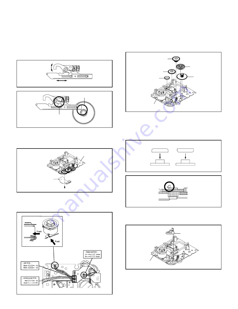
2-9: GEAR (Refer to Fig. 2-9-A)

1.
2.

Unlock the support 

1

.

Remove the Middle Gear 1/2/3, Idler Gear and Feed Gear.

Middle Gear 2

Middle Gear 1

Middle Gear 3

Feed Gear

Idler Gear

Main Chassis Ass’y

Fig. 2-9-A

NOTE

1.

2.

In case of the Idler Gear installation, install correctly as
Fig. 2-9-B.
When installing the Middle Gear 2, check if the Middle
Gear 2 is locked correctly as Fig. 2-9-C.

Fig. 2-9-B

Fig. 2-9-C

NOTE

1.

2.

After the assembly of the Rack Feed, check if the Rack
Feed 1/2 is moving smoothly. (Refer to Fig. 2-7-B)
In case of the Rack Feed Ass’y installation, install cor-
rectly as Fig. 2-7-C.

Moving smoothly

Moving smoothly

Fig. 2-7-B

Should not be engaged.

Check the position of
the Rack Feed Lever.

Fig. 2-7-C

2-8: RELAY PCB ASS’Y (Refer to Fig. 2-8-A)

1.
2.

Remove the screw 

1

.

Remove the Relay PCB Ass’y.

Main Chassis Ass’y

Relay PCB Ass’y

• Screw Torque: 4 

±

 0.5kgf•cm

1

Fig. 2-8-A

[OK]

Idler Gear

Idler Arm

[NG]

Idler Gear

Idler Arm

Check Lock

Middle Gear 2

NOTE

1. When installing the wire of the Relay PCB, install it

correctly as Fig. 2-8-B.

Fig. 2-8-B

2-10: IDLER ARM (Refer to Fig. 2-10)

Remove the Idler Arm.

1.

Fig. 2-10

Idler Arm

Main Chassis Ass'y

Summary of Contents for MD13P1C

Page 1: ...SERVICE MANUAL COLOR TELEVISION DVD VIDEO PLAYER MD13P1C FILE NO 140 200419 ...

Page 2: ...e a ground conductive wrist strap for body Location of the required Marking The rating sheet and the safety caution are on the rear of the unit CERTIFICATION COMPLIES WITH FDA RADIATION PERFORMANCE STANDARDS 21 CFR SUBCHAPTER J CAUTION THIS DIGITAL VIDEO PLAYER EMPLOYS A LASER SYSTEM TO ENSURE PROPER USE OF THIS PRODUCT PLEASE READ THIS SERVICE MANUAL CARE FULLY AND RETAIN FOR FUTURE REFERENCE SHO...

Page 3: ...itions or whether there are the portions which are deteriorated around the serviced places serviced or not Check the insulation between the antenna terminal or external metal and the AC cord plug blades And be sure the safety of that INSULATION CHECK PROCEDURE 1 2 3 4 Unplug the plug from the AC outlet Remove the antenna terminal on TV and turn on the TV Insulation resistance between the cord plug...

Page 4: ...al power company For units intended to operate from battery power or other sources refer to the operating instructions GROUNDING OR POLARIZATION This unit is equipped with a polarized alternating current line plug a plug having one blade wider than the other This plug will fit into the power outlet only one way This is a safety feature If you are unable to insert the plug fully into the outlet try...

Page 5: ... equipment turn off the power and unplug all of the equipment from the wall outlet Failure to do so may cause an electric shock and serious personal injury Read the owner s manual of the other equipment carefully and follow the instructions when making any connections SOUND VOLUME Reduce the volume to the minimum level before you turn on the product Otherwise sudden high volume sound may cause hea...

Page 6: ...A DISCHARGE UNIT NEC SECTION 810 20 ANTENNA LEAD IN WIRE GROUNDING CONDUCTORS NEC SECTION 810 21 GROUND CLAMPS POWER SERVICE GROUNDING ELECTRODE SYSTEM NEC ART 250 PART H GROUND CLAMP ELECTRIC SERVICE EQUIPMENT NEC NATIONAL ELECTRICAL CODE S2898A IMPORTANT SAFEGUARDS CONTINUED ...

Page 7: ...ing To unlock the Tray Lock please follow the steps below NB The above procedure will reset ALL of the player s settings to the default factory state Turn Unit ON Set the DVD to the Stop Mode Set the VOLUME to minimum Press and hold the VOL DOWN button on the front panel Simultaneously press and hold the 4 key on the remote control unit Hold both keys for more than 1 second The On Screen Display m...

Page 8: ...D CIRCUIT BOARDS DVD AV CRT RELAY SW SCHEMATIC DIAGRAMS MPEG MICON MEMORY RF AMP DSP AUDIO VIDEO REGULATOR MICON TUNER VIF SIF CHROMA SOUND AMP IN OUT STEREO DEFLECTION CRT POWER RELAY SW FG INTERCONNECTION DIAGRAM WAVEFORMS MECHANICAL EXPLODED VIEWS DVD DECK EXPLODED VIEW MECHANICAL REPLACEMENT PARTS LIST DVD DECK PLACEMENT PARTS LIST ELECTRICAL REPLACEMENT PARTS LIST A1 1 A1 2 A1 2 A1 3 A1 5 A1 ...

Page 9: ... 40 times CD Rev 2 20 times 4 step Actual 2 45 times DVD VIDEO CD 4 40 times CD Slow speed Fwd 1 7 1 2 times Actual Rev 1 7 1 2 times Actual G 3 Tuning Broadcasting System US System M System Tuner and System 1Tuner Receive CH Destination US w CATV Tuning System F Synth Input Impedance VHF UHF 75 Ohm CH Coverage 2 69 4A A 5 A 1 A I J W W 1 W 84 Intermediate Picture FP 45 75MHz Frequency Sound FS 41...

Page 10: ...rage 20oC 60oC G 8 Operating Humidity Less than 80 RH G 9 On Screen Menu TV Yes Display Menu Type Icon TV Setup Yes Picture Yes Audio No Picture Preference Yes Channel Setup Yes TV CATV Yes Auto CH Memory Yes Add Delete Yes V chip Setup No Language Yes Sleep Timer Yes CH AV LINE DVD Yes Stereo Audio Output Yes Bilingual No SAP Yes Control Volume Yes Level Bright Contrast Sharpness Color Yes Tint Y...

Page 11: ...s TV Screen Size Yes OSD Display On Off Yes JPEG Interval Yes Select Files No Sound Yes DRC Dynamic Range Control Yes dts Decode No Output 5 1ch 2ch No Surround On Off No Center On Off No Sub Woofer On Off No Parental Yes Password Lock Un Lock Yes Rating Level Yes Other Yes OSD Language Set up Language Yes Output RGB Composite No A3 3 ...

Page 12: ... Title No Yes Angle No Yes Vocal On Off Yes Audio No Yes Audio Stereo L R Yes Video CD Zoom Yes Marker No No Program Play Back Yes CD VIDEO CD JPEG Surround On Off No Screen Saver No JPEG Folder Name Yes File Name Yes File No Yes Time No Track No Yes G 11 OSD Language TV English French Spanish DVD English French Spanish G 12 Clock and Sleep Timer Max Time 120 Min Timer Step 10 Min On Off Timer Pro...

Page 13: ...s Play Yes Stop Yes Search Yes Search Yes Skip Yes Skip Yes Slow Yes Slow Yes Pause Yes Call Yes TV DVD Yes Cancel Yes Audio Select Yes Angle Yes Subtitle Yes Top Menu Yes Set up Menu Yes DVD Menu Yes Return Yes Up Set CH Up Yes Down Set CH Down Yes Left Select Vol Down Yes Right Select Vol Up Yes Select Enter Yes Play Mode Yes Closed Caption Yes Input Select Yes Repeat A B Yes Zoom Quick View Yes...

Page 14: ... Leak Circuit Yes Choke Coil No Power On Memory No Tray Lock Yes Parental Lock DVD Only Yes Video CD Playback Yes SVCD Playback No Overlay Graphics And Text No Command List No Entry Point Jump No MP3 Playback No WMA Playback No JPEG Playback Yes Digital Out Dolby Digital Yes MPEG Yes PCM Yes DTS Yes Down Mix Out Dolby Digital Yes DTS No Surround Tru Surround No Screen Saver No Picture Preference Y...

Page 15: ... Information Return No G 16 Interface Switch Front Power Tact Yes Channel Up Yes Channel Down Yes Volume Up Yes Volume Down Yes Play Yes Open Close Yes Skip Yes Skip Yes Still Pause No Stop Yes Main Power SW No Rear Main Power SW No Indicator Power Yes Red Stand by No On Timer No Terminals Front Video Input RCA x 1 Audio Input RCA x 2 Stereo Other Terminal Head Phone Rear Video Input No Audio Inpu...

Page 16: ...nsions W x D x H mm 423x447x443 Design As Per Buyer s Description of Origin Yes Drop Test Natural Dropping At 1 Corner 3 Edges 6 Surfaces Height cm 62 Container Stuffing 40 container 700 Sets G 20 Material Cabinet Front PS 94V0 DECABROM Rear PS 94V0 DECABROM Jack Panel PCB Non Halogen Demand No Eyelet Demand Yes G 21 Environment Pb Free Lead free Solder No Other No Cd Free No A3 8 ...

Page 17: ...op Shield in the direction of arrow A Disconnect the following connectors CP8001 and CP8002 Remove the 4 screws 2 Remove the DVD Block in the direction of arrow B Remove the screw 3 Remove the Jack Shield Remove the AV PCB in the direction of arrow C Fig 1 4 1 2 CRT PCB Refer to Fig 1 2 CAUTION BEFORE REMOVING THE ANODE CAP DISCHARGE ELECTRICITY BECAUSE IT CONTAINS HIGH VOLTAGE BEFORE ATTEMPTING T...

Page 18: ...nnectors CP2601 CP2602 and CP2603 Remove the 4 screws 2 Remove the DVD Deck in the direction of arrow B Remove the 4 screws 3 Remove the DVD PCB in the direction of arrow C 1 5 DVD PCB DVD DECK Refer to Fig 1 5 Fig 1 5 When the installation of the DVD Deck remove all the soldering on the short circuit position after the connection of Pick Up PCB and DVD PCB connector NOTE DVD PCB DVD Deck Deck Ang...

Page 19: ...r R Green 1 Main Frame Ass y Main Chassis Ass y 2 4 CLAMPER ASS Y INSULATOR R LEVER SWITCH Refer to Fig 2 4 A 1 2 3 4 5 Remove the screw 1 Remove the Lever Switch Remove the 2 Insulator R Press the Clamper and rotate the Clamper Plate clockwise then unlock the 3 supports 2 Remove the Clamper Plate Clamper Magnet and Clamper Insulator R Green Insulator R Green Clamper Plate Clamper Magnet Main Fram...

Page 20: ... D Fig 2 4 B Fig 2 4 C Fig 2 4 D 2 5 TRAVERSE HOLDER INSULATOR F Refer to Fig 2 5 A 1 2 Remove the Traverse Holder Remove the 2 Insulator F Main Chassis Ass y Insulator F Black Traverse Holder Insulator F Black Fig 2 5 A Lever Switch Blue White Red From DVD PCB NOTE 1 After the installing of the Traverse Holder check if the wire is like Fig 2 5 B 2 6 SWITCH PCB ASS Y Refer to Fig 2 6 A Remove the ...

Page 21: ...k if the Rack Feed 1 2 is moving smoothly Refer to Fig 2 7 B In case of the Rack Feed Ass y installation install cor rectly as Fig 2 7 C Moving smoothly Moving smoothly Fig 2 7 B Should not be engaged Check the position of the Rack Feed Lever Fig 2 7 C 2 8 RELAY PCB ASS Y Refer to Fig 2 8 A 1 2 Remove the screw 1 Remove the Relay PCB Ass y Main Chassis Ass y Relay PCB Ass y Screw Torque 4 0 5kgf c...

Page 22: ... 1 1 Motor Gear Feed Motor Main Chassis Ass y NOTE 1 2 In case of the Motor Gear installation check if the value of the Fig 2 11 B is correct When installing the Feed Motor check if the cable is positioned as Fig 2 11 C Fig 2 11 B 6 1 0 1mm Safety surface for pressing of the insert Feed Motor Motor Gear Fig 2 11 C Main Chassis Ass y Feed Motor Pass the cable between 2 pins ...

Page 23: ...ip up the sides of the Rubber Cap in the direction of the arrow and remove one side of the support Refer to Fig 3 2 2 GND on the CRT Screwdriver Alligator Clip Support CRT GND on the CRT Rubber Cap CRT Support Fig 3 1 Fig 3 2 3 After one side is removed pull in the opposite direction to remove the other NOTE DISASSEMBLY INSTRUCTIONS INSTALLATION 1 Clean the spot where the cap was located with a sm...

Page 24: ...ring the IC leads completely Fig 4 2 Blower type IC desoldering machine IC 3 When IC starts moving back and forth easily after desoldering completely pickup the corner of the IC using a tweezers and remove the IC by moving with the IC desoldering machine Refer to Fig 4 3 NOTE Some ICs on the PCB are affixed with glue so be careful not to break or damage the foil of each IC leads or solder lands un...

Page 25: ...eld Wire Refer to Fig 4 7 NOTE Do not absorb the solder to excess Fig 4 7 Soldering Iron IC Braided Shield Wire 4 When bridge soldering between terminals and or the soldering amount are not enough resolder using a Thin tip Soldering Iron Refer to Fig 4 8 Fig 4 8 Thin tip Soldering Iron IC 5 Finally confirm the soldering status on four sides of the IC using a magnifying glass Confirm that no abnorm...

Page 26: ...E Do not use this for the normal servicing If you set a factory initialization the memories are reset such as the channel setting and the POWER ON total hours POWER ON total hours are displayed on the screen Refer to the PREVENTIVE CHECKS AND SERVICE INTERVALS CONFIRMATION OF HOURS USED Can be checked of the INITIAL DATA of MEMORY IC Refer to the WHEN REPLACING EEPROM MEMORY IC Initialization of t...

Page 27: ...required ADDRESS to be changed is reached Press ENTER to select DATA When DATA is selected it will blink Again step through the DATA using VOL UP DOWN button until required DATA value has been selected Pressing ENTER will take you back to ADDRESS for further selection if necessary Repeat steps 4 to 7 until all data has been checked When satisfied correct DATA has been entered turn POWER off return...

Page 28: ... CENT COL DVD MAX COL DVD MIN TINT DVD SHARPNESS DVD SUB BIAS BRI GAME CENT BRI GAME MAX BRI GAME MIN CONT GAME CENT CONT GAME MAX CONT GAME MIN SUB BIAS TUNING V MUTE POWER ON V MUTE INPUT LEVEL SEPARATION L SEPARATION H X RAY TEST H STOP H FREQ BAST WEST DC BAST WEST AMP BAST WEST TILT BAST WEST COR TOP BAST WEST COR BOT H SIZE COMP H BLK L AV H BLK R AV NO 39 40 41 42 43 44 45 46 47 48 49 50 51...

Page 29: ... a broadcast and check if the picture is normal 2 8 VERTICAL LINEARITY 1 2 3 4 NOTE Receive the monoscope pattern Using the remote control set the brightness and contrast to normal position Activate the adjustment mode display of Fig 1 1 and press the channel button 09 on the remote control to select VLIN Press the VOL UP DOWN button on the remote control until the SHIFT quantity of the OVER SCAN ...

Page 30: ...e display of Fig 1 1 and press the channel button 42 on the remote control to select BRTCD Press the VOL UP DOWN button on the remote control to set the same step numbers as the AV Press the GAME button on the remote control to set to the GAME mode Activate the adjustment mode display of Fig 1 1 and press the channel button 54 on the remote control to select BRTCG Press the VOL UP DOWN button on t...

Page 31: ... NO 2A 40 10 70 10 10 00 70 2A 40 10 00 00 40 3F 00 00 00 00 00 00 07 05 2 15 CONTRAST MAX 1 2 3 4 5 6 7 8 9 10 11 12 13 Activate the adjustment mode display of Fig 1 1 and press the channel button 22 on the remote control to select CNTX Press the VOL UP DOWN button on the remote control until the contrast step No becomes 5A Receive a broadcast and check if the picture is normal Press the INPUT SE...

Page 32: ...s between the deflection yoke and CRT funnel to fix the deflection yoke Refer to Fig 3 2 b R G B R G B Fig 3 2 a WEDGE WEDGE WEDGE WEDGE POSITION Fig 3 2 b R G B R G B Receive the crosshatch pattern from the color bar generator Combine red and blue of the 3 color crosshatch pattern on the center of the screen by adjusting the pair of 4 pole magnets Combine red blue magenta and green by adjusting t...

Page 33: ...CD2301 CD2001 CD2302 DVD DECK SPEAKER SPEAKER AC IN CRT CRT CRT PCB J801 CP802B CP803B TP024 TP022 TU001 J4201 VR3800 CP803A TP401 FB401 CP3800 CP401 VR401 CP302 CP101 CP802A CP8002 CP8001 CP301 J2202 J2203 J2204 J2201 AV PCB CP8502 CD4002 CP2601 CP2602 CP2601 CD805 CD803 CD802 CD301 CD8501 CD302 S3801 S3802 ...

Page 34: ...NS VCR BLOCK TX RX P CON 3 3V CD DVD LD RFA_SDEN DATA SCLK EEPROM IC4002 AT24C04N 10SI 2 7 CD4002 RF AAF_CE FE TE PI FNN FNP VBIASS0 S1 DEFECT LINK MIRR LDON HOME TIN SW TOUT SW TR FO SPDL SLED SPINDLE SLED_PWM TRACK FOCUS_DAC ADC IN 5 6 7 S MUTE HA0 HA20 HD0 HD15 SDA0 SDA11 I CDAT 2 I CCLK 2 P CON 5V P CON 9V SPDIF DVD RESET CP8502 DVD AUDIO L DVD AUDIO R ZERO STEREO DAC IC8502 PCM1742KEG 2K DVD ...

Page 35: ...A 18 17 22 23 24 A 26 27 36 33 1 2 RESET IC103 PST3231NR A BUFFER STOP SKIP FF OPEN CLOSE PLAY VOL UP VOL DOWN CH UP 32 31 X101 16MHz TV BLOCK DIAGRAM 38 4 37 SOUND DECORDER IC902 AN5829S 19 18 22 21 J2202 FROM DVD BLOCK DVD C DVD Y DVD_A_OUT_L AMP IC4201 NJM4580M TE1 5 3 Q4209 Q4212 MUTE SW L R D Q4203 MUTE ZERO E A AT 5 6V B P CON 9V C CHROMA 5V D P CON A5V E P CON 12V 1 7 POWER ON OFF SKIP REW ...

Page 36: ...DJ IC3800 PS2561L1 1 V W FB401 2 3 1 5V REG IC3001 KIA7805API 3 1 5V REG IC3002 KIA7805API 3 1 9V REG IC3005 KIA7809API P CON 3 3V OUT Q3003 Q3004 Q3007 POWER BLOCK DIAGRAM P CON 3 3V P CON D5V AT 5 6V SOUND B P CON D9V P CON 9V POWER ON H B POWER FEED BACK P CON 5V 10 DVD_H P CON 12V DRIVE Q3005 DRIVE Q3000 SW Q3001 DRIVE Q3008 DRIVE Q3010 E 5 E 6 ...

Page 37: ...R4013 C4042 C4092 B4006 C4066 C4065 C4097 W874 R2651 R2650 R2652 R2653 R2649 R2626 C2642 C2616 R4022 C2647 B2602 R2621 C4013 C2303 R2304 C2306 C2301 B4007 C4095 C4039 W854 W802 C4077 C4082 W855 W860 W832 C4037 C4081 C4094 C4093 C4098 C4038 C4026 R4053 R4054 R4014 R4035 R4031 IC4002 B8502 B8503 B4005 W833 IC8502 Q8502 Q8503 Q8504 C8505 C8506 C8509 C8508 C8512 C8511 B4003 B4001 R4052 W857 C4001 C400...

Page 38: ...2 D3831 R3813 R3829 R414 W043 W015 R402 D405 W012 CP803A Q3010 R3010 C3021 IC3005 C3026 R3001 C3820 C3015_1 Q3008 W009 W010 C3013_1 C3030 C3808 W820 W007 W005 D3803 D408 C3023_2 C3014_1 R614 W037 W038 W036 W033 C634 D603 C605 R3830 TP403 TP402 D409 W197 C410 D416 D410 W001 R802_1 R806_1 TP023 TP022 R807 R803 TP024 R805 PH3800 T3800 FB401_1 D3804 IC302 W041 W042 W813 W222 W110 TU001 R412 C110_1 W02...

Page 39: ...28 C124 R106 R109 R304 C117 R147 R143 C310 IC4201 IC103 R122 C2202 C2203 C4274 C4266 C331 I C 6 0 1 R306 R307 C306 R113 R121 R813 C809 R815 R809 R801 R808 C811 R816 C810 C632 C631 C625 C629 C630 R626 C627 R624 R625 C621 R619 R617 C620 C618 R615 C613 C617 C614 R611 R610 R609 R602 C608 R608 C607 R607 Q601 R628 C944 R420 C4224 C002 C001 C4205 Q4201 R4216 C4215 C3806 Q3007 R634 Q602 C3809 R4208 C3805 ...

Page 40: ...PRINTED CIRCUIT BOARDS F 7 F 8 CP1 S1002X S1003X S1005X S1004X S1001X RELAY INSERTED PARS SOLDER SIDE RELAY CHIP MOUNTED PARS SOLDER SIDE 0 0 SW2 SW SOLDER SIDE 0 0 2 0 02 S1005Y S1004Y ...

Page 41: ...SEL HA8 LINK HA12 TRAY_OPEN HA9 MIRR HA10 HD15 TOUT_SW LDON HA11 SMUTE HA11 TRAY_CLOSE HA12 TRACK_DAC HD7 TIN_SW HA13 FOCUS_DAC SMUTE HA14 SPINDLE_PWM HA15 HA10 SLED_PWM HA16 P CON A5V HD14 HA17 P CON 3 3V HA9 HA18 VCC 9V HD6 HA19 P CON 5V HA20 HA8 RESET ADCIN_7 HD0 ADCIN_6 HD13 HD1 ADCIN_5 HD5 HD2 M_GND HA20 HOME HOME HD3 D_GND HD4 LDON GND HD5 HD12 HD6 WR DJTDO ML HD7 HD4 DJTDI MC DUPTD1 HD8 HD9...

Page 42: ...D_D10 SD_D5 RAMCS0 HD12 HA20 RAMCS1 SD_D9 SD_D6 RAMRAS RAMCAS HD4 WR SD_BA0 RAMDQM SD_D8 SD_D7 RAMWE RESET RAMCLK HA0 HA1 HD11 RAMDQM HA2 HA3 RAMDQM RAMWE HA4 HD3 HA5 RAMCLK RAMCAS HA6 HA7 HD10 HA19 RAMRAS HA8 HA9 RAMCS1 HA10 HD2 HA18 HA11 SD_A11 SD_BA0 HA12 HA13 HD9 HA17 SD_A9 RAMCS0 HA14 HA15 SD_A8 SD_A10 HA16 HD1 HA7 HA17 SD_A7 SD_A0 HA18 HA19 HD8 HA6 SD_A6 SD_A1 HA20 HD0 SD_A5 SD_A2 HD1 HD0 HA...

Page 43: ...0 22K R2629 1 5K R2628 22K R2619 100 R2621 100 R2622 4 7K R2647 4 7K R2624 4 7K R2623 4 7K R2617 1K R2618 18 R2331 470 R2344 1 2 1 2W R2345 1 2 1 2W R2646 2 2K R2625 4 7K R2627 1 5K R2626 4 7K R2316 20K R2309 470 B2601 FCM2012H 102T04 B2602 FCM2012H 102T04 B2604 FCM2012H 102T04 B2603 FCM2012H 102T04 B2605 FCM2012H 102T04 W864 W863 W861 W808 W807 W806 W862 W875 W882 OF PRINTING AND SUBJECT TO CHANG...

Page 44: ...74 W873 W871 W876 W879 W877 OF PRINTING AND SUBJECT TO CHANGE WITHOUT NOTICE NOTE THIS SCHEMATIC DIAGRAM IS THE LATEST AT THE TIME DURING PLAYBACK MEASURED WITH THE DIGITAL TESTER NOTE THE DC VOLTAGE EACH PART WAS L8504 1uH 0305 L8502 1uH 0305 L8503 1uH 0305 DAC_C C _VIDEO DAC_B Y _VIDEO P CON A5V P CON A5V DAC_D_DVD_VIDEO DAC_VIDEO_C DAC_VIDEO_B DAC_VIDEO_D P CON 5V P CON 3 3V RESET DAC_VIDEO_C M...

Page 45: ...2W R3004 1K 1 4W R3006 10K 1 4W R3018 1K 1 4W R3010 1M 1 4W R3001 100 1 4W W803 W850 W852 W819 W857 Q3005 KTC3209_Y DRIVER Q3008 KTC3203_Y DRIVER Q3009 KTC3209_Y DRIVER Q3007 KTC3875S_Y_RTK SW Q3003 KTC4369 3 3V OUT Q3006 KTC3203_Y DRIVER OF PRINTING AND SUBJECT TO CHANGE WITHOUT NOTICE NOTE THIS SCHEMATIC DIAGRAM IS THE LATEST AT THE TIME DURING PLAYBACK MEASURED WITH THE DIGITAL TESTER NOTE THE ...

Page 46: ...K R141 2 7K R145 2 7K R106 4 7K R109 4 7K R113 4 7K R121 4 7K R119 10K R123 10K R143 100 R160 2 2K R159 33K 1 4W R190 10K 1 4W W805 W828 W837 W863 W814 W812 W804 W856 Q105 KTC3875S_Y_RTK V BUFFER OF PRINTING AND SUBJECT TO CHANGE WITHOUT NOTICE NOTE THIS SCHEMATIC DIAGRAM IS THE LATEST AT THE TIME L001 100uH 9A06B SCL SDA I2C_OFF REMOCON KEY_A KEY_B POWER_ON_H TUNER_AUDIO TUNER_VIDEO POWER_FAIL P ...

Page 47: ...618 220 1 4W R628 10K W809 W827 W832 W849 Q602 KTC3875S_Y_RTK SW Q601 KTC3875S_Y_RTK SW OF PRINTING AND SUBJECT TO CHANGE WITHOUT NOTICE NOTE THIS SCHEMATIC DIAGRAM IS THE LATEST AT THE TIME L602 100uH 9A06B L601 100uH 0305 X601 100CT3R505 3 579545MHz DVD_C P CON 5V SYNC_VIDEO FRONT_VIDEO POWER_ON_H P CON 5V_B DVD_Y DVD_C UNREG 12V P CON 5V GND P CON 9V SWD_V_OUT AT5 7VREG 8 5VREG V OUT ACL AFC H ...

Page 48: ...0V YK C346 2 2 50V KA C347 2 2 50V KA C307 0 01 B C348 0 01 B C331 0 1 B C323 0 1 B C304 470P CH C305 470P CH C303 470P CH C302 470P CH C310 0 001 B C306 0 001 B C328 4 7 50V KA R346 4 7K 1 4W R311 270K R302 68K R307 4 7K R301 2 2K 1 4W R309 1K R304 820 R306 820 R308 1K R310 1K R303 2 2K 1 4W R305 1K R323 47K 1 4W R326 100 B301 W4BRH3 5X6X1 0 W813 Q301 KTC3875S_Y_RTK MUTE Q305 KTC3875S_Y_RTK BUFFE...

Page 49: ... 3K R4252 100 1 4W R4237 10K R4228 12K R4223 10K R4233 1K R4219 1K 1 4W R4211 100K R4212 100K R4213 10K R4224 10K R4208 10K R4229 12K R4236 10K R4251 100 1 4W R4210 220 R4216 68 R4205 2 2K 1 4W R4239 1K R4240 1K 1 4W R4241 1 5K R4234 100 1 4W R4209 4 7K R4243 10K R4235 100 1 4W R4238 3 3K R4231 10K R4218 1K 1 4W R4232 10K R4221 100K R4202 10K R4201 10K R4230 1K R2226 100 1 4W R2221 5 6K R2220 2 7K...

Page 50: ...910 220K W833 W823 W842 W834 W815 W844 OF PRINTING AND SUBJECT TO CHANGE WITHOUT NOTICE NOTE THIS SCHEMATIC DIAGRAM IS THE LATEST AT THE TIME L902 100uH 0305 L904 100uH TUNER_AUDIO SCL SDA A_OUT_L A_OUT_R P CON 12_A A_O_R A_O_L DVD_AUDIO_L DVD_AUDIO_R FRONT_A_IN_R FRONT_A_IN_L P CON 12V P CON 5V GND PCB250 TMB555 FROM REGULATOR FROM IN OUT TO SOUND AMP FROM TO MICON TUNER Filter SAPout 75us De Emp...

Page 51: ... CURRENT DET C418 22 50V YK C421 470 35V MHE D414 1N4005 EIC D413 1N4937 D401 11E1 EIC D405 1SS133 D406 1SS133 D409 1SS133 C439 56P 500V SL C430 0 001 500V B C417 0 01 100V MMTS C428 0 0086 1 25KV MPP C423 0 39 250V PMS C429 0 0022 500V B C432_1 0 47 100V MKT C434_1 0 22 100V MKT C401 10 250V YK C422 2 2 250V MHE C407 2200 25V YK C405 1 50V YK C406 100 35V YK C431 22 250V YK C402 22 100V YK C403 4...

Page 52: ...ES PAR UN ETANT ATTENTION SINCE THESE PARTS MARKED BY CAUTION DESCRIBED IN PARTS LIST ONLY CRITICAL FOR SAFETY USE ONES ARE R SIGNAL B SIGNAL D801 1SS133 D802 1SS133 D803 1SS133 C811 390P CH C809 470P CH C810 390P CH C802 0 001 2KV B R813 270 R816 270 R815 270 R804 2 7K 1 4W R808 4 7K R809 4 7K R801 4 7K R802_1 2 7K 1 4W R806_1 2 7K 1 4W Q804 2SC4217 RED AMP Q806 2SC4217 BLUE AMP Q805 2SC4217 GREE...

Page 53: ... 2200 25V MHE C3815 470 200V UP C3823 1000 25V MHE C3822 2200 16V MHE C3826 220 200V YXF C3820 10 50V KA D3818 1N4937 D3816 RM11C EIC D3826 1SS133 D3815 RM11C EIC D3808 RM11C EIC D3819 21DQ09N D3827 1SS133 D3822 1SS133 D3823 SB340L 6737 D3817 SB340L 6737 D3820 21DQ09N D3809 RM11C EIC D3821 RU2AM EIC D3830 21DQ09N D3803 1SS133 D3802 1SS133 D3805 1SS133 D3807 1N4937 D3806 1N4937 B EIC D3811 1SS133 C...

Page 54: ...JECT TO CHANGE WITHOUT NOTICE NOTE THIS SCHEMATIC DIAGRAM IS THE LATEST AT THE TIME M M2002 BCD3B02 M M2001 JCL9B61 D1 SG 107F6 1 2 3 4 R2 82K R1 560 S1002X S1001X S1004X S1003X S1005X S1002Y S1001Y S1004Y S1003Y S1005Y SW2 SW1AB 271 10A CP1 IMSA 9615S 08C PP 1 2 3 4 5 6 7 8 RELAY SW FG SCHEMATIC DIAGRAM RELAY PCB SW PCB AWD28 S1002 S1003 S1001 S1004 S1005 VCC FG GND L SW SP MTR SLD MTR SLD MTR SP...

Page 55: ... ANODE NC NC HEATER GND 180V SCREEN FOCUS J801_1 9 8 7 6 5 4 3 F CRT SOCKET 1 NC 180V HEATER GND SCREEN G OUT CLAMP GND R OUT B OUT CLAMP OFF G OUT GND CLAMP CLAMP_OFF B OUT R OUT CRT PCB PCB110 GND GND V801 H V CRT WHITE RED YELLOW SP OUT L SP OUT R SP OUT R 8 OHM 8 OHM SP OUT L TM101 FROM OS2201 TO REMOCON SENSOR COMMAND TRANSMITTER TM101 B V OUT GND NC NC NC NC NC NC NC NC NC NC VMC319 VREF MON...

Page 56: ...iagram NOTE MICON TUNER 22 23 24 25 26 POWER ON 0 2ms 1 0V POWER ON 0 2ms 1 0V POWER ON 0 2ms 1 0V POWER ON 5ms 1 0V POWER ON 50µs 1 0V 1 2 3 6 8 7 MPEG MICON 4 200ns 500mV 9 100µs 200mV 10ns 100mV 100ns 100mV 5ns 200mV 500µs 500mV 10µs 200mV 500µs 500mV MEMORY RF AMP DSP AUDIO VIDEO 5 10 10µs 100mV 200ns 100mV H 1 ...

Page 57: ...OUT 27 28 29 NOTE 30 31 32 36 37 33 34 35 38 39 40 STEREO 41 POWER ON 20µs 0 5V STANDBY 0 5µs 50mV POWER ON 10µs 2 0V POWER ON 10µs 2 0V POWER ON 10µs 2 0V POWER ON 20µs 0 5V POWER ON 20µs 2 0V POWER ON 1ms 100mV POWER ON 1ms 100mV POWER ON 1ms 200mV POWER ON 1ms 50mV DVD PLAY 10µs 0 5V DVD PLAY 0 5ms 200mV POWER ON 10ms 0 5V DVD PLAY 0 5ms 200mV H 2 ...

Page 58: ...point of the corresponding balloon number in the schematic diagram NOTE POWER DEFLECTION 47 48 49 46 44 45 43 42 POWER ON 1ms 200mV POWER ON 5ms 10 0V POWER ON 20µs 5 0V POWER ON 20µs 50V POWER ON 20µs 50V STANDBY 5µs 5 0V STANDBY 5µs 5 0V POWER ON 20µs 50V H 3 ...

Page 59: ...114 116 202 202 102 202 202 206 I1 1 201 201 201 201 118 PCB110 CRT PCB ASS Y 117 121 117 MECHANICAL EXPLODED VIEW 101 A 101F 101C 101D 101A 101E 115 210 210 210 210 101B 129 106 ...

Page 60: ...04 204 204 211 211 207 107 109 206 203 203 A 108 208 208 208 208 208 208 208 208 208 208 110 112 208 208 103 MECHANICAL EXPLODED VIEW I1 2 PCB130 DVD PCB ASS Y 120 209 209 209 113 209 209 104 208 205 205 205 208 112 208 208 119 208 208 205 ...

Page 61: ...MECHANICAL EXPLODED VIEW PACKING DIAGRAM I1 3 125 122 124 124 124 124 123 127 128 BL001 TM101 123 123 123 130 ...

Page 62: ... 610 604 602 AA AA 605 601 605 703 PCB640 SW PCB ASS Y CD2001 CD2301 Do not replace the parts Because minute adjustments are needed if this condition is disassembled further more If the repair is needed replace the DVD MECHA ASS Y CP1 SW2 AA 608 Applying positions AA for the grease are displayed for this section Check if the correct grease is applied for each position NOTE CLASS GREASE MARK AA ...

Page 63: ...NO 117 AD302158 800WR0A002 SHEET CRT SUPPORT 118 BZ710660 741WUA0021 SPRING EARTH 119 AE003764 899EFBA001 WIRING CLIP 120 AE002846 752WSA0384 ANGLE DVD 2 121 AE004123 723000C589 POP LABEL 122 AE002901 791WHDA001 LAMIFILM BAG 123 AD301669 792WHA0412 PACKAGE TOP 124 AE004114 792WHAA121 PACKAGE BOTTOM 125 AE004124 793WCDC234 GIFT BOX 126 AE004125 A5K303V975 INSTRUCTION BOOK KIT 127 AE002695 JB5UD100 ...

Page 64: ... 92P100082A CLAMPER 2 618 AD301839 92P300002A SPRING RACK LOADING 619 AD301840 92P400002A MAGNET CLAMPER 620 AD301847 92P100030A GEAR IDLER 621 AD301842 92P100025A GEAR MOTOR 622 AE002180 92P100083A GEAR MIDDLE 1 623 AD301844 92P100027A GEAR MIDDLE 2 701 BZ710187 8110226804 SCREW TAP TITE P BIND 2 6x8 702 AD301851 8110120604 SCREW TAP TITE P PAN 2x6 703 AD301852 8107220504 SCREW TAP TITE S BIND 2x...

Page 65: ... 0 0047UF 250V C3818 BZ110101 E5EZF3222M CE 2200 UF 25V C3820 BZ110188 E50HU5100M CE 10 UF 50V C3822 BZ110129 E5EZF2222M CE 2200 UF 16V C3823 BZ110032 E5EZF3102M CE 1000 UF 25V C3826 BZ110130 E62NFC221M CE 220 UF 200V C3827 BZ110101 E5EZF3222M CE 2200 UF 25V DIODES D101 BZ410006 D1VT001330 DIODE SILICON 1SS133T 77 D102 BZ410021 D97U05R61B DIODE ZENER MTZJ5 6B T 77 D103 BZ410021 D97U05R61B DIODE ZE...

Page 66: ...E004116 I03FC319N0 IC LA76319NM MPB E IC902 BZ611068 I01FF58290 IC AN5829S IC2301 BZ611126 I03F065600 IC LA6560 IC2601 AE002837 ICQK067080 IC ZR36708TQC IC2602 AD301770 I07E00358F IC BA10358F E2 IC3001 BZ611015 I1KA97805A IC KIA7805API IC3002 BZ611015 I1KA97805A IC KIA7805API IC3005 BZ611033 I1KA97809A IC KIA7809API IC3800 AD301771 000220001W PHOTO COUPLER PS2561L1 1 V W IC4001 AE000842 ICQK067620...

Page 67: ... L902 BZ310041 02167F101J COIL 100 UH L904 BZ310041 02167F101J COIL 100 UH L3000 AD301785 02167E100K COIL R6 1 10 UH L3001 AD301785 02167E100K COIL R6 1 10 UH L3800 BZ310076 028R140031 COIL DEGAUSS 8R140031 L3801 AD301786 029T000110 COIL LINE FILTER 1R1A223F28 L3803 AD301539 02AHB0A0A4 CORE FERRITE W5T_20 10 10A L4001 BZ310191 02167F2R2J COIL 2 2 UH L4002 BZ310118 02AHB9A972 CORE FERRITE W5T29X7 5...

Page 68: ...301 BZ614268 069W120029 CONNECTOR PCB SIDE TID X02P M1 CP302 BZ614268 069W120029 CONNECTOR PCB SIDE TID X02P M1 CP401 BZ614303 069S450089 CONNECTOR PCB SIDE A1561WV2 A5P CP801 BZ614269 069S320010 CONNECTOR PCB SIDE A2361WV2 2P CD3800 BZ614341 120R414903 CORD AC BUSH 0R414903 CD4002 BZ614299 06CU2B2001 CORD CONNECTOR CU2B2001 CD8501 AD301792 122H0C1001 CORD JUMPER 2H0C1001 CP2601 AD302396 069JYOT09...

Page 69: ...RBON RESISTOR CAPACITORS CC CERAMIC CAPACITOR CE ALUMI ELECTROLYTIC CAPACITOR CP POLYESTER CAPACITOR CPP POLYPROPYLENE CAPACITOR CPL PLASTIC CAPACITOR CMP METAL POLYESTER CAPACITOR CMPL METAL PLASTIC CAPACITOR CMPP METAL POLYPROPYLENE CAPACITOR J3 5 ...

Page 70: ...TOSHIBA CORPORATION 1 1 SHIBAURA 1 CHOME MINATO KU TOKYO 105 8001 JAPAN ...

Reviews: