background image

1-13-15

E9KGASCD4

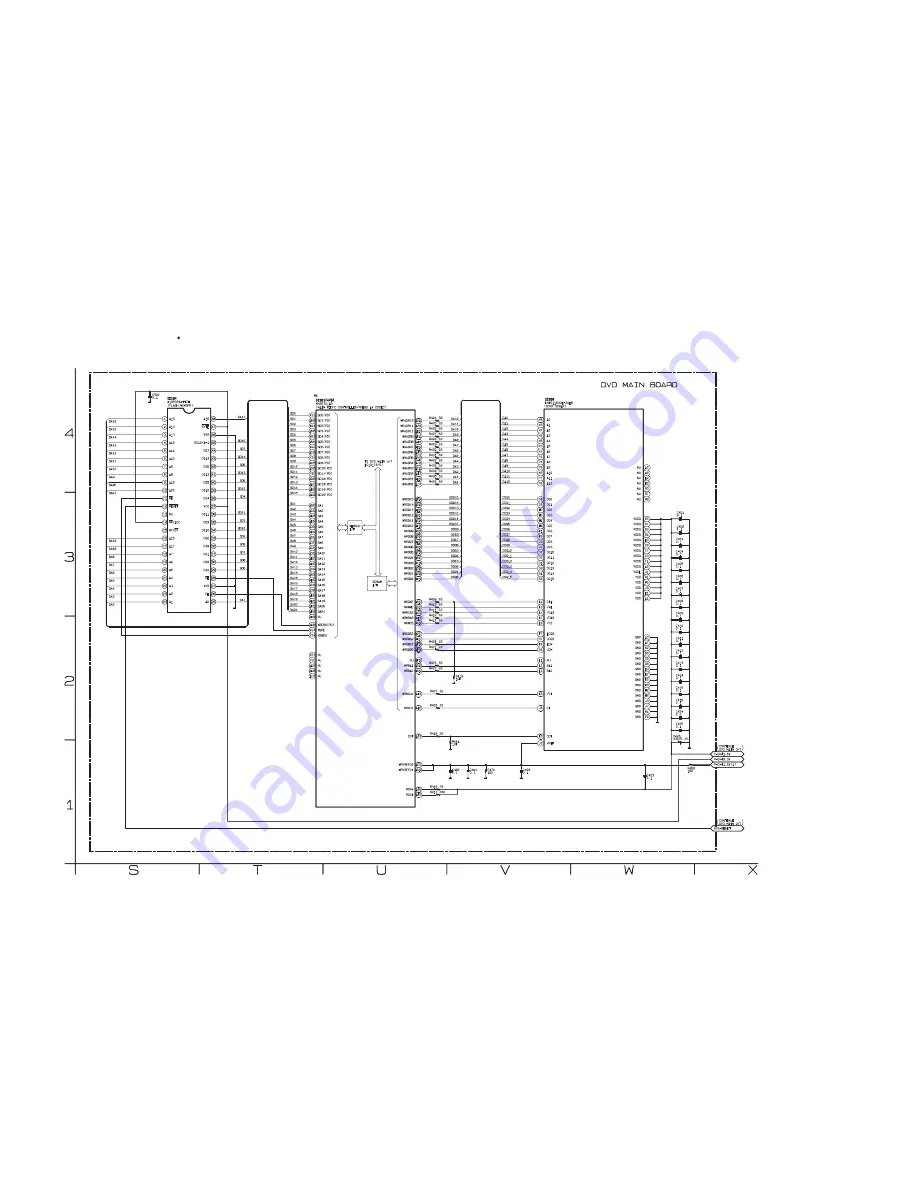
DVD MAIN 4/7 Schematic Diagram < DVD Section >

NOTE: BOARD MEANS PRINTED CIRCUIT BOARD.

The order of pins shown in this diagram is different from that of actual IC101.
IC101 is divided into six and shown as IC101 (1/6) ~ IC101 (6/6) in this DVD Main Schematic Diagram Section.

1   NOTE:

Summary of Contents for D-VR610KU

Page 1: ...ed serial number This Service Manual describes replacement parts for the green product When repairing this green product use the part s described in this manual and lead free solder 2 For 1 and 2 see the next page FILE NO 810 200803GR DVD Video Recorder Video Cassette Recorder D VR610KU Published in Japan Jan 2008 GREEN ...

Page 2: ...ent of parts is not only confined to manufacture The same green parts used in manufacture must also be used as replacement parts 2 LEAD FREE SOLDER This product is manufactured using lead free solder as a part of a movement within the consumer products industry at large to be environmentally responsible Lead free solder must be used in the servicing and repair of this product WARNING This product ...

Page 3: ...oting 1 10 1 Function Indicator Symbols 1 11 1 Block Diagrams 1 12 1 Schematic Diagrams BOARD s and Test Points 1 13 1 Waveforms 1 14 1 Wiring Diagram VCR Section 1 15 1 Wiring Diagram DVD Section 1 15 2 IC Pin Function Descriptions 1 16 1 Lead Identifications 1 17 1 Exploded Views 1 18 1 Mechanical Parts List 1 19 1 Electrical Parts List 1 20 1 Main Section I Specifications I Preparation for Serv...

Page 4: ...1 rear Input 1 rear 2 front L R Jacks RCA jack S video output Y luminance Output level 1 Vp p 75Ω C color Output level 286 mVp p 75Ω Jack 4 pin mini DIN Audio input During audio input 2 V rms input impedance more than 22 kΩ Jacks RCA jacks Component video output Output level Y 1 0 Vp p 75Ω PB CB PR CR 0 7 Vp p 75Ω Digital audio output Output level 500 mVp p 75Ω Jack RCA jack Note The specification...

Page 5: ...way from the pickup lens when the diode is turned on Do not look directly at the laser beam CAUTION Use of controls and adjustments or doing procedures other than those specified herein may result in hazardous radiation exposure Location Inside Top of DVD mechanism Do not look directly at the laser beam coming from the pickup or allow it to strike against your skin Drive Mechanism Assembly Laser B...

Page 6: ...ical for safety Replace only with part number specified B In addition to safety other parts and assemblies are specified for conformance with regulations applying to spurious radiation These must also be replaced only with specified replacements Examples RF converters RF cables noise blocking capacitors and noise blocking filters etc C Use specified internal wiring Note especially 1 Wires covered ...

Page 7: ...lug prongs and externally exposed accessible parts RF terminals antenna terminals video and audio input and output terminals microphone jacks earphone jacks etc is lower than or equal to the specified value in the table below Measuring Method Power ON Insert load Z between B earth ground power cord plug prongs and exposed accessible parts Use an AC voltmeter to measure across the terminals of load...

Page 8: ...air to the Flat Pack IC about 5 to 6 seconds Fig S 1 1 2 Remove the flat pack IC with tweezers while applying the hot air 3 Bottom of the flat pack IC is fixed with glue to the BOARD when removing entire flat pack IC first apply soldering iron to center of the flat pack IC and heat up Then remove glue will be melted Fig S 1 6 4 Release the flat pack IC from the BOARD using tweezers Fig S 1 6 CAUTI...

Page 9: ...y one using a sharp pin or wire to which solder will not adhere iron wire When heating the pins use a fine tip soldering iron or a hot air desoldering machine Fig S 1 4 3 Bottom of the flat pack IC is fixed with glue to the BOARD when removing entire flat pack IC first apply soldering iron to center of the flat pack IC and heat up Then remove glue will be melted Fig S 1 6 4 Release the flat pack I...

Page 10: ... Fig S 1 6 Note When using a soldering iron care must be taken to ensure that the flat pack IC is not being held by glue When the flat pack IC is removed from the BOARD handle it gently because it may be damaged if force is applied 2 Installation 1 Using desoldering braid remove the solder from the foil of each pin of the flat pack IC on the BOARD so you can install a replacement flat pack IC more...

Page 11: ... to remove any static electricity that may be charged on the body 2 Ground for Workbench Be sure to place a conductive sheet or copper plate with proper grounding 1 MΩ on the workbench or other surface where the semi conductors are to be placed Because the static electricity charge on clothing will not escape through the body grounding band be careful to avoid contacting semi conductors with your ...

Page 12: ...to the Deck Mechanism Assembly and press the O VCR button The tape will be loaded into the Deck Mechanism Assembly Make sure the power is on connect TP502 S INH to GND This will stop the function of Tape Start Sensor Tape End Sen sor and Reel Sensors If these TPs are connected before plugging in the unit the function of the sensors will stay valid See Fig 1 Note Because the Tape End Sensors are in...

Page 13: ...racket D3 S 5 5 BOARD Front Jack D3 Jack Plate Earth 6 DVD Mechanism DVD Main BOARD Assembly D4 4 S 6 S 6a S 7 CN101 CN701 CN901 Mecha Plate Earth R 4 7 Dust Cover D4 8 Panel Rear Unit D5 3 S 8 6 S 9 CN1102 1 Cover Top 2 Panel Front 3 Front Bracket 4 Jack Bracket 5 BOARD Front Jack 6 DVD Mechanism DVD Main BOARD Assembly 8 Panel Rear Unit 12 BOARD Power Supply 10 Motor DC Fan 13 BOARD Holder 11 Pa...

Page 14: ...eck Assembly while aligning the hole of Cam Gear with the pin of LD SW the shaft of Cam Gear with the hole of LD SW as shown in Fig D9 4 The DVD Mechanism DVD Main BOARD Assembly is adjusted as a unit at factory Therefore do not disassemble it Replace the DVD Mechanism DVD Main BOARD Assembly as a unit S 1 S 1 S 1 1 Cover Top Fig D1 L 1 S 3 S 3 S 4 S 2 L 2 L 1 L 1 2 Panel Front 3 Front Bracket CN1...

Page 15: ...1102 8 Panel Rear Unit Fig D6 11 Panel Rear 10 Motor DC Fan 9 Fan Holder S 10 Fig D7 S 12 S 12 S 11 S 11 12 BOARD Power Supply 13 BOARD Holder CN1101 Plate Earth Fig D8 S 13 S 17 S 18 S 15 S 14 S 14 S 16 Board Washer S 14 14 VCR Chassis Unit ...

Page 16: ... 18 BOARD Main SW1512 LD SW From FE Head BOTTOM VIEW Lead connections of Deck Assembly and BOARD Main Desolder From Capstan Motor Assembly Printing side Desolder From Cylinder Assembly From ACE Head Assembly Lead with blue stripe Lead with blue stripe Desolder Lead with black stripe S 19 S 20 Desolder Lead with blue stripe Fig D9 LD SW Pin Hole Hole Shaft Cam Gear 15 Deck Assembly Pin ...

Page 17: ...1 6 5 E9KGADC Fig D10 19 Deck Pedestal 20 Front Bracket R S 21 S 21 S 21 S 21 S 23 S 22 DV Plate Earth DV Jack ...

Page 18: ...the Front Bracket 4 Remove the DVD Mechanism DVD Main BOARD Assembly 5 Unhook two places and detach the Dust Cover 6 Rotate the gear in the direction of the arrow manually as shown below until the tray descends 7 Pull the tray out manually and remove a disc View for A Rotate this gear in the direction of the arrow Hook Front Bracket Panel Front Dust Cover A ...

Page 19: ...ge DC AC 20MHz 2 Alignment Tape FL8A Head Switching Position Adjustment Purpose To determine the Head Switching position during playback Symptom of Misadjustment May cause Head Switching noise or vertical jitter in the picture Reference Notes Playback the Alignment tape and adjust VR1501 so that the V sync front edge of the CH1 video output waveform is at the 6 5H 1H 416μs 64μs delayed position fr...

Page 20: ...n the initializing is completed the DVD recorder exits the Version display mode and turns off the power automatically To move into the Normal mode from the Version display mode press RETURN button on the remote control unit instead of ENTER button When button is pressed before ENTER button is pressed the DVD recorder exits the Version display mode then the power turns off MODEL NAME FE VERSION BE ...

Page 21: ...scribed as follows 5 After updating is finished the tray opens automatically At this time no button is available 6 Pull out the AC code once then insert it again Fig a Version Up Mode Screen Firmware Version differs depending on the models and this indication is one example Current F W version is displayed Firm Update Mode Please insert a disc ver WL5T H1E Fig b VFD in Version Up Mode Fig c Update...

Page 22: ...pler circuit operate normally Check the circuit and replace P3 BOARD POWER SUPPLY if defective IC1010 D1006 D1010 D1029 Check the circuit and replace P3 BOARD POWER SUPPLY if defective IC1010 Q1031 D1017 D1025 D1036 FLOW CHART NO 4 When buzz sound can be heard in the vicinity of power circuit Check if there is short circuit on the rectifying diode and the circuit in each rectifying circuit of seco...

Page 23: ... is not outputted Is 12V voltage supplied to the collector of Q1055 No No Yes Yes Is 10V voltage supplied to the base of Q1055 Check D1014 D1017 C1012 and their periphery and replace P3 BOARD POWER SUPPLY if defective FLOW CHART NO 8 AL 18V is not outputted Is the supply voltage 44V fed the cathode of D1013 No Yes Check D1083 R1092 R1095 and their periphery and replace P1 BOARD MCV if defective Ch...

Page 24: ...D1015 D1016 C1017 C1019 L1012 and their periphery and replace P3 BOARD POWER SUPPLY if defective Yes Yes Yes Yes No No No No FLOW CHART NO 13 The fluorescent display tube does not light up Is 5V voltage supplied to Pin 6 24 of IC1571 Is approximately 24V to 28V voltage supplied to Pin 15 of IC1571 Is there approximately 500kHz oscillation to Pin 26 of IC1571 Are the filament voltage applied betwee...

Page 25: ...85 of IC1501 Replace P2 DVD MECHANISM DVD MAIN BOARD ASSEMBLY Replace P1 BOARD MCV if defective No FLOW CHART NO 2 Replace P1 BOARD MCV Or replace remote control unit X1 Check the line between the RS1501 remote control receiver and the Pin 5 of IC1501 and replace P1 BOARD MCV if defective Is the L pulse sent out from Pin 1 terminal of the RS1501 remote control receiver when the remote control unit...

Page 26: ...f IC2805 Yes No No IC2805 VIDEO IN 1 REAR 8PIN IC2805 Y IN 1 REAR 13PIN IC2805 VIDEO Y CVBS 19PIN IC2805 VIDEO C 21PIN CN2201 VIDEO Y CVBS 20PIN CN2201 VIDEO C 22PIN VIDEO Y CVBS 20PIN VIDEO C 22PIN IC2805 C IN 1 REAR 2PIN IC2805 VIDEO IN 2 FRONT 10PIN VIDEO IN 1 REAR Y IN 1 REAR C IN 1 REAR VIDEO IN 2 FRONT IC2805 JK2804 8PIN IC2805 JK2401 13PIN IC2805 CN2201 19PIN IC2805 CN2201 21PIN Check the l...

Page 27: ... the COMPONENT OUT terminal JK2403 Are the luminance signals outputted to the S VIDEO OUT terminal JK2402 Are the chroma signals outputted to the S VIDEO OUT terminal JK2402 No No No No No Are the composite video signals outputted to the VIDEO OUT terminal JK2751 Is the video signal outputted to Pin 15 of IC2406 Is the video signal outputted to the emitter of Q2391 Check the line between the emitt...

Page 28: ...ace P1 BOARD MCV if defective Are the video signals outputted to the specific output terminal Are the Y Pb Cb Pr Cr signals outputted to the COMPONENT OUT terminal JK2403 Are the luminance signals outputted to the S VIDEO OUT terminal JK2402 Are the chroma signals outputted to the S VIDEO OUT terminal JK2402 No No No No No Are the composite video signals outputted to the VIDEO OUT terminal JK2751 ...

Page 29: ...DIO L OUT CN2201 15PIN AUDIO R OUT IC2804 1PIN AUDIO L OUT IC2804 7PIN AUDIO R OUT IC2804 2PIN AUDIO L OUT IC2804 6PIN AUDIO R OUT Replace P1 BOARD MCV Check the periphery between Pin 1 7 of IC2804 and the audio terminal JK2805 and replace P1 BOARD MCV if defective Check each line between each pin of CN2201 and each pin of IC2804 and replace P1 BOARD MCV if defective CN2201 17PIN IC2804 2PIN AUDIO...

Page 30: ... and each pin of IC2804 and replace P1 BOARD MCV if defective CN2201 17PIN IC2804 2PIN AUDIO L OUT CN2201 15PIN IC2804 6PIN AUDIO R OUT Are the analog audio signals inputted to each pin of IC2804 Are the analog audio signals outputted to each pin of IC2804 Are the audio signals outputted to the specific output terminal Are the audio signals outputted to the audio terminal JK2805 Are the audio sign...

Page 31: ... 61 1 98 2 39 2 90 3 60 4 30 D V OUTPUT CH UP CH DOWN FF REC OTR PLAY REW STOP EJECT POWER Terminal voltage of IC1501 86 KEY 1 IC1501 86 V Replace P1 BOARD MCV Or replace remote control unit X1 Check the line between the RS1501 remote control receiver and the Pin 5 of IC1501 and replace P1 BOARD MCV if defective Is the L pulse sent out from Pin 1 terminal of the RS1501 remote control receiver when...

Page 32: ...e signal inputted to Pin 3 of IC1501 While the reel pulse signal is inputting is L pulse inputted to Pin 26 of IC1501 Is the specified voltage approximately 13V outputted to the terminal of the Lading Motor Unit When loading a cassette tape does the LD SW operate normally When loading a cassette tape is the specified voltage approximately 13V outputted to the terminal of the Loading Motor Unit Che...

Page 33: ...tween Pin 8 of CN1502 and Pin 34 of IC1501 and replace P1 BOARD MCV if defective Check the AL 12V 1 line and replace P1 BOARD MCV or P3 BOARD POWER SUPPLY if defective Check the AL 12V 1 line and replace P1 BOARD MCV or P3 BOARD POWER SUPPLY if defective DRUM PG FG SIGNAL WAVEFORM Replace P1 BOARD MCV No No No No No No No No No No No Yes Yes Yes Is 5V voltage supplied to Pin 2 of CN1502 Is the dru...

Page 34: ... of IC2101 and replace P1 BOARD MCV if defective Is the video signal inputted into Pin 1 of IC2101 No Check the AL 5V AL 5V line and replace P1 BOARD MCV if defective Is 5V voltage supplied to Pin 16 of IC2101 Is 5V voltage supplied to Pin 7 of IC2101 Check the line between Pin 22 23 24 of IC2805 and Pin 57 58 59 of IC1501 and replace P1 BOARD MCV if defective Replace P1 BOARD MCV Replace P1 BOARD...

Page 35: ...n 7 69 of IC1451 Yes Check the line between Pin 3 13 of IC2801 and Pin 7 69 of IC1451 and replace P1 BOARD MCV if defective No No No IC2801 AUDIO IN1 REAR 4 11PIN IC2801 AUDIO IN2 FRONT 5 14PIN AUDIO IN1 REAR AUDIO IN2 FRONT IC2801 JK2804 4 11PIN Are active level of Pin 9 10 of IC2801 become as shown below IC2801 JK1232 JK1233 5 14PIN INPUT LINE REAR LINE FRONT 9PIN 10PIN H H L H Continued to D on...

Page 36: ...eplace P1 BOARD MCV if defective Check the line between Pin 4 14 of IC2406 and the audio output terminal JK2751 and replace P1 BOARD MCV if defective Replace P1 BOARD MCV Is the L pulse inputted into the Pin 49 of IC1451 Is the H pulse inputted into the Pin 9 10 11 of IC2101 Is the audio signal outputted to Pin 4 14 of IC2406 Yes No No No Is 5V voltage supplied to Pin 16 of IC2406 or 5V voltage su...

Page 37: ...Yes Is the audio signal outputted to Pin 9 of IC1301 Yes Yes No No Check the line between Pin 6 of IC1451 and Pin 76 78 80 of IC1301 and replace P1 BOARD MCV if defective Check the Bias oscillation circuit Q1421 Q1422 Q1425 Q1426 and replace P1 BOARD MCV if defective No Replace P1 BOARD MCV No FLOW CHART NO 15 Audio can not be playbacked normally in the linear audio mode E E mode is normal Is ther...

Page 38: ...n reel or capstan mechanism is not functioning correctly A R is displayed on a TV screen Refer to Fig 1 When tape loading mechanism is not func tioning correctly A T is displayed on a TV screen Refer to Fig 2 When cassette loading mechanism is not functioning correctly A C is displayed on a TV screen Refer to Fig 3 When the drum is not working properly A D is displayed on a TV screen Refer to Fig ...

Page 39: ...dable 14 Cannot write the data after recovering SMALL VMGI 15 Cannot write the data after DVD R Reverse Track 16 An error occurs in Finalize Close 17 An error occurs in Rec Stop Close 18 An error occurs in PCA Full DVD_R 19 Safety Stop occurs during editing 20 High Speed Disc 2 21 The disc is not formatted 5 22 Disc Error has occurred 3 23 The R Disc of VR Mode 6 24 The disc except for finalized D...

Page 40: ...38 Sector Address is wrong 39 BUP writing error of chapter editing You cannot record more than 49 titles on one disc The maximum is 49 Delete unnecessary titles 43 The 49 titles has been reached VR Format 9 You cannot record more than 254 chapters on one disc The maximum is 254 Delete unnecessary chapter marks 44 The 254 chapter has been reached VR Format Disc 10 This program is not recordable in ...

Page 41: ...IO BLOCK DIAGRAM TO Hi Fi AUDIO BLOCK DIAGRAM TO POWER SUPPLY BLOCK DIAGRAM IIC BUS SDA IIC BUS SCL 17 18 IIC BUS SCL IIC BUS SDA NORMAL L 78 Hi Fi H SW Hi Fi NOR IN Hi Fi H SW 30 OUTPUT SELECT OUTPUT SELECT2 OUTPUT SELECT OUTPUT SELECT2 DISPLAY DATA 7 DISPLAY CLK CLK 1G 2G 4G 5G 6G 7G 3G GRID SEGMENT VFD STB DIN 8 REMOTE 5 REMOTE SENSOR RS1501 FL1501 2 28 1 21 22 23 18 17 19 20 9 8 7 12 13 14 16 ...

Page 42: ... FWD REV 26 D CONT 34 DECK ASSEMBLY END S T REEL T REEL ST S ST S Q1504 Q1503 Q1506 SW POINT AL 5V 1 VR1501 TP506 TP505 END S TP507 SW1511 REC SW LD SW 87 AL 12V AL 5V 1 AL 5V 1 SW1512 AL 18V P ON 5V 1 MODE SW AL 5V D1555 S LED 5 CTL 6 CTL 1 AL 12V 1 2 P ON 5V 1 3 C FG 4 C F R 5 C CONT 6 GND 7 LM FWD REV 8 D CONT 9 D PFG 10 GND 11 AL 12V 12 AL 18V TP513 CTL AL 12V 1 BOARD MAIN CAPSTAN MOTOR CYLIND...

Page 43: ... CONTROLLER MPEG2 AV CODEC R4 TO VIDEO INPUT SELECT BLOCK DIAGRAM TO VIDEO OUTPUT SELECT BLOCK DIAGRAM CN1001 SPINDLE MOTOR M CN1002 CN301 P ON 3 3V VIDEO Y CVBS VIDEO C IC701 VIDEO DECODER DECODER A D 45 50 U4 W1 W3 Y2 AA1 AA2 A5 B5 B7 C6 C7 D6 D7 DECODER A D 39 44 P3 T3 T5 U2 U3 V1 10 8 13 M5 VIDEO Y I D A HDMI SDA HDMI SCL HDMI SDA HDMI SCL YC 0 7 N23 U25 SPDIF SPDIF PCM BCK PCM LRCK PCM SCLK P...

Page 44: ...O INPUT SELECT BLOCK DIAGRAM TO VIDEO OUTPUT SELECT BLOCK DIAGRAM VCR VIDEO DVD VIDEO DUB VCR DVD TO SYSTEM CONTROL BLOCK DIAGRAM CYLINDER ASSEMBLY RF SW RF SW 59 V ENV H A SW H A COMP H A COMP TP302 VIDEO L 2 HEAD VIDEO R 2 HEAD TP301 C PB D V SYNC C SYNC D V SYNC 25 53 24 YCA SCL 14 36 37 39 34 Q1301 BUFFER 30 58 60 SP EP 54 YCA SDA 55 YCA CS SERIAL I F VCA CLAMP 69 70 SP HEAD AMP EP HEAD AMP 72...

Page 45: ...EO IN1 REAR JK2804 VIDEO IN2 JK1231 13 19 2 12 10 8 21 CN2609 CN1231 22 23 24 VIDEO SW2 TO SYSTEM CONTROL BLOCK DIAGRAM VIDEO SW3 BOARD FRONT JACK CONTROL LOGIC BUFFER BUFFER BUFFER LPF LPF DVD MAIN BOARD CN701 20 20 VIDEO Y CVBS IN 22 22 VIDEO C IN CN2201 VCR VIDEO TO VIDEO BLOCK DIAGRAM Q2304 BUFFER Q2305 BUFFER VCR VIDEO DUB TO VIDEO BLOCK DIAGRAM VIDEO SW1 VCR DVD DUBBING 20 VIDEO Y CVBS VIDEO...

Page 46: ...MAIN BOARD CN701 7 7 VIDEO Y I P OUT 9 9 VIDEO C OUT 3 3 VIDEO Pb Cb OUT 5 5 VIDEO Pr Cr OUT VIDEO Y I P VIDEO C VIDEO Pb Cb VIDEO Pr Cr JK2402 REAR S VIDEO OUT CN2201 3 4 2 1 IC2405 VIDEO DRIVER 4dB AMP 2dB AMP LPF DRIVER Y C IC2406 OUTPUT SELECT 11 4dB AMP 2dB AMP LPF DRIVER 6 10 4dB AMP 2dB AMP LPF DRIVER 8 VIDEO Pb Cb OUT VIDEO Y OUT VIDEO Pr Cr OUT JK2403 REAR VIDEO OUT COMPOSITE JK2751 REAR ...

Page 47: ...PF 10 SP LP ON P R ALC AUDIO SIGNAL PROCESS 76 80 78 TUNER LINE 1 LINE 2 4 AUDIO PB REC CN1504 3 A COM 1 AE H 2 AE H FE H AUDIO HEAD AUDIO ERASE HEAD AC HEAD ASSEMBLY FE HEAD DECK ASSEMBLY 1 FE H 2 FE H GND CN1501 BOARD MAIN PB AUDIO SIGNAL REC AUDIO SIGNAL 58 55 53 54 D REC AUDIO MUTE TO SYSTEM CONTROL BLOCK DIAGRAM FULL ERASE HEAD YCA CS YCA SCL YCA SDA IC1301 N A OUT N A IN TO Hi Fi AUDIO BLOCK...

Page 48: ...H IN1 EE EE IN2 R CH SW CTL AUDIO SW2 AUDIO SW1 OUTPUT SELECT2 TO SYSTEM CONTROL BLOCK DIAGRAM SW CTL SW CTL OP AMP IC2804 OUTPUT SELECT IC2406 2 6 1 7 JK2751 REAR AUDIO L OUT2 AUDIO R OUT2 TO SYSTEM CONTROL BLOCK DIAGRAM TO Hi Fi AUDIO BLOCK DIAGRAM CN2609 CN1231 REC AUDIO SIGNAL PB AUDIO SIGNAL 12 13 5 3 14 4 TP754 A OUT L WF10 WF9 9 10 11 DVD MAIN BOARD 3 3 SPDIF 17 17 AUDIO L OUT 15 15 AUDIO R...

Page 49: ... AUDIO L DVD AUDIO R LIM 49 LINE L OUT LINE R OUT N A IN Hi Fi H SW AUDIO MUTE NORMAL L TO AUDIO BLOCK DIAGRAM IIC BUS SDA IIC BUS SCL P ON 9V TO SYSTEM CONTROL BLOCK DIAGRAM BOARD MAIN Hi Fi AUDIO R 7 Hi Fi COM 8 Hi Fi AUDIO L 9 CN1253 IC1451 MTS SAP Hi Fi AUDIO PROCESS Hi Fi HEAD AMP REC AUDIO SIGNAL PB AUDIO SIGNAL Mode SP REC TO AUDIO BLOCK DIAGRAM TO SYSTEM CONTROL BLOCK DIAGRAM TO SYSTEM CON...

Page 50: ...LP NOTE BOARD MEANS PRINTED CIRCUIT BOARD A V AC1001 F1001 1A 250V LINE FILTER L1001 D1001 D1004 BRIDGE RECTIFIER 2 4 Q1001 Q1003 Q1008 8 7 3 4 IC1010 ERROR VOLTAGE DET HOT COLD T1001 Q1055 Q1052 Q1102 Q1103 BOARD POWER SUPPLY BOARD MAIN F HOT CIRCUIT BE CAREFUL 20 19 18 17 16 15 14 13 12 11 1 1 AL 44V 2 2 AL 12V 1 3 3 AL 12V 2 4 AL 12V 2 5 DVD 5V 8 AL 5V 17 AL 30V 19 AL 2 8V 20 AL 2 8V 25 AL 4V 2...

Page 51: ... diagram and the parts list Before replacing any of these components read the parts list in this manual carefully The use of substitute replacement parts that do not have the same safety characteristics as specified in the parts list may create shock fire or other hazards Notes 1 Do not use the part number shown on these drawings for ordering The correct part number is shown in the parts list and ...

Page 52: ...use only original replacement parts which are listed with their part numbers in the parts list section of the service manual 4 Voltage indications for PLAY and REC mode on the schematics are as shown below 5 How to read converged lines 6 Test Point Information A V F This symbol means fast operating fuse Ce symbole represente un fusible a fusion rapide REC mode 2 3 1 5 0 2 5 PLAY mode 5 0 The same ...

Page 53: ...1 13 3 E9KGASCM1 MAIN 1 7 Schematic Diagram VCR Section NOTE BOARD MEANS PRINTED CIRCUIT BOARD ...

Page 54: ...c e a b d f g c e a b d f g c e a b d f g c e a b FL1501 MATRIX CHART PM BS CS DR CD VCR DB HDD DVD DTV T C PM DTV BS CS CD VCR HDD DVD DR DB T C 5G 4G 3G 2G 1G 7G 6G a S1 b c d e f g MAIN 2 7 POWER SWITCH DVD OPEN CLOSE SWITCH SENSOR Schematic Diagram VCR Section NOTE BOARD MEANS PRINTED CIRCUIT BOARD ...

Page 55: ...1 13 5 E9KGASCM3 MAIN 3 7 Schematic Diagram VCR Section NOTE BOARD MEANS PRINTED CIRCUIT BOARD ...

Page 56: ...1 13 6 E9KGASCM4 MAIN 4 7 Schematic Diagram VCR Section NOTE BOARD MEANS PRINTED CIRCUIT BOARD ...

Page 57: ...1 13 7 E9KGASCM5 MAIN 5 7 Schematic Diagram VCR Section NOTE BOARD MEANS PRINTED CIRCUIT BOARD ...

Page 58: ...1 13 8 E9KGASCM6 MAIN 6 7 Schematic Diagram VCR Section NOTE BOARD MEANS PRINTED CIRCUIT BOARD ...

Page 59: ...1 13 9 E9KGASCM7 MAIN 7 7 Schematic Diagram VCR Section NOTE BOARD MEANS PRINTED CIRCUIT BOARD ...

Page 60: ... the AC plug to the AC power supply Otherwise it may cause some components in the power supply circuit to fail NOTE The voltage for parts in hot circuit is measured using hot GND as a common terminal Ce symbole reprèsente un fusible à fusion rapide CAUTION For continued protection against fire hazard replace only with the same type fuse ATTENTION Pour une protection continue les risqes d Incele n ...

Page 61: ...1 13 11 E9KGASCFJ FRONT JACK Schematic Diagram VCR Section NOTE BOARD MEANS PRINTED CIRCUIT BOARD ...

Page 62: ...agram DVD Section NOTE BOARD MEANS PRINTED CIRCUIT BOARD The order of pins shown in this diagram is different from that of actual IC101 IC101 is divided into six and shown as IC101 1 6 IC101 6 6 in this DVD Main Schematic Diagram Section 1 NOTE ...

Page 63: ...agram DVD Section NOTE BOARD MEANS PRINTED CIRCUIT BOARD The order of pins shown in this diagram is different from that of actual IC101 IC101 is divided into six and shown as IC101 1 6 IC101 6 6 in this DVD Main Schematic Diagram Section 1 NOTE ...

Page 64: ...agram DVD Section NOTE BOARD MEANS PRINTED CIRCUIT BOARD The order of pins shown in this diagram is different from that of actual IC101 IC101 is divided into six and shown as IC101 1 6 IC101 6 6 in this DVD Main Schematic Diagram Section 1 NOTE ...

Page 65: ...agram DVD Section NOTE BOARD MEANS PRINTED CIRCUIT BOARD The order of pins shown in this diagram is different from that of actual IC101 IC101 is divided into six and shown as IC101 1 6 IC101 6 6 in this DVD Main Schematic Diagram Section 1 NOTE ...

Page 66: ...agram DVD Section NOTE BOARD MEANS PRINTED CIRCUIT BOARD The order of pins shown in this diagram is different from that of actual IC101 IC101 is divided into six and shown as IC101 1 6 IC101 6 6 in this DVD Main Schematic Diagram Section 1 NOTE ...

Page 67: ...1 13 17 E9KGASCD6 DVD MAIN 6 7 Schematic Diagram DVD Section NOTE BOARD MEANS PRINTED CIRCUIT BOARD ...

Page 68: ...agram DVD Section NOTE BOARD MEANS PRINTED CIRCUIT BOARD The order of pins shown in this diagram is different from that of actual IC101 IC101 is divided into six and shown as IC101 1 6 IC101 6 6 in this DVD Main Schematic Diagram Section 1 NOTE ...

Page 69: ... SW POINT VR1501 CTL TP513 RF SW TP302 WF2 C PB TP301 WF3 V OUT TP751 WF1 S INH TP502 BOARD MAIN Top View BOARD SENSOR Top View BHF300F01012B BHF300F01012A NOTE BOARD MEANS PRINTED CIRCUIT BOARD BE9MG0F01011A ...

Page 70: ...2 OF IC2406 WF6 PIN 3 OF CN2204 WF10 PIN 5 OF CN2201 WF8 PIN 3 OF CN2201 WF7 PIN 17 OF CN2201 WF9 PIN 9 OF CN2201 WF5 PIN 7 OF CN2201 WF4 BOARD MAIN Bottom View BE9MG0F01011A NOTE BOARD MEANS PRINTED CIRCUIT BOARD ...

Page 71: ...ent in the power supply circut an isolation transformer must be used Also in order to have the ability to increase the input slowly when troubleshooting this type power supply circuit a variable isolation transformer is required CAUTION Fixed voltage or Auto voltage selectable power supply circuit is used in this unit If Main Fuse F1001 is blown check to see that all components in the power supply...

Page 72: ...esent in the power supply circut an isolation transformer must be used Also in order to have the ability to increase the input slowly when troubleshooting this type power supply circuit a variable isolation transformer is required CAUTION Fixed voltage or Auto voltage selectable power supply circuit is used in this unit If Main Fuse F1001 is blown check to see that all components in the power supp...

Page 73: ...MG0F01011B BOARD DVD OPEN CLOSE SWITCH Top View BOARD DVD OPEN CLOSE SWITCH Bottom View BOARD FRONT JACK Top View BOARD FRONT JACK Bottom View BOARD POWER SWITCH Top View BOARD POWER SWITCH Bottom View NOTE BOARD MEANS PRINTED CIRCUIT BOARD ...

Page 74: ...V 0 1μs WF10 Pin 3 of CN2204 WF4 Pin 7 of CN2201 VIDEO Y 0 2V 20μs WF5 Pin 9 of CN2201 VIDEO C 0 2V 20μs WF6 Pin 2 of IC2406 VIDEO CVBS 0 5V 20μs NOTE Input COLOR BAR SIGNAL WITH 1KHz AUDIO SIGNAL WF3 WF1 UPPER WF2 WF2 LOWER TP751 TP302 UPPER LOWER TP302 TP301 V OUT 0 5V 50μs RF SW 5V C PB RF SW 5V 5ms 0 2V WF1 TP751 V OUT E E 0 2V 20μs WL5NWF ...

Page 75: ... Fi AUDIO R Hi Fi COM Hi Fi AUDIO L VIDEO COM VIDEO R 2 VIDEO COM VIDEO L 2 VIDEO L 1 VIDEO R 1 AL 12V 1 P ON 5V 1 C F R C FG C CONT GND LM FWD REV D CONT D PFG GND AL 12V AL 18V FE H FE H GND AE H AE H FE H A COM AUDIO PB REC CTL CTL 18 AL 2 8V AL 30V 17 GND 15 GND 14 GND 13 GND 12 GND 11 GND 10 GND 9 AL 5V 8 DVD 5V 7 DVD 5V 6 DVD 5V 5 AL 12V 2 4 AL 12V 2 3 AL 12V 1 2 AL 44V 1 GND 16 FAN 1 LOADIN...

Page 76: ...1 8V 6 GND 9 GND 5 GND 4 P ON 3 3V 17 P ON 3 3V 16 P ON 3 3V 15 GND 28 GND 29 GND 30 DVD MAIN BOARD DVD MECHANISM PICKUP BOARD RELAY CN201 CN1001 10 8 HW 9 9 HW 1 FCS 4 TRK 3 TRK 2 FCS 6 TILT 5 TILT 7 LDD IIN4 9 LDD IIN2 10 LDD IINR 11 TH 8 LDD IIN3 12 LDD VDD 14 LDD ENABLE 15 LDD OSCEN 16 GND 17 LDD WEN4 18 GND 19 LDD WEN3 20 GND 21 LDD WEN2 22 LDD SEL1 23 PD VC 24 PD VSW 25 F 26 G 27 H 28 E 29 R...

Page 77: ...Switching Pulse 24 OUT D V SYNC Dummy V sync Output 25 IN RESET System Reset Signal Reset L 26 OUT LM FWD REV Loading Motor FWD REV Output 27 OUT P ON L Power On Signal to Low 28 NU Not Used 29 OUT D REC Delayed Record Signal 30 OUT Hi Fi H SW Hi Fi Audio Head Switching Pulse 31 OUT VCR AUDIO MUTE VCR Audio Mute Control Signal 32 OUT C F R Capstan Motor FWD REV Control Signal FWD L REV H 33 OUT C ...

Page 78: ...POWER SAFETY DVD Power Supply Safety Signal 80 IN VCR POWER SAFETY VCR Power Supply Safety Signal 81 IN END S Tape End Position Detect Signal 82 NU Not Used 83 IN V ENV Video Envelope Comparator Signal 84 IN PG DELAY Video Head Switching Pulse Signal Adjusted Voltage 85 IN KEY 2 Key Data Input 2 86 IN KEY 1 Key Data Input 1 87 IN LD SW Deck Mode Position Detector Signal Pin No IN OUT Signal Name F...

Page 79: ...e 3 NU Not Used 4 NU Not Used 5 VSS Ground 6 VDD Power Supply 7 OUT P9 Segment Output 8 P8 9 P1 10 P2 11 P3 12 P4 13 P5 14 P6 15 VEE Pull Down Level 16 OUT P7 Segment Output 17 OUT 7G Grid Output 18 6G 19 5G 20 4G 21 3G 22 2G 23 1G 24 VDD Power Supply 25 VSS Ground 26 IN OSC Oscillator Input 27 NU Not Used 28 IN DIN Serial Data Input ...

Page 80: ...e A Anode K Cathode E Emitter C Collector B Base R Reference S Source G Gate D Drain 2SK3563 Q CD4053BNSR PT204 6B 12 RN1511 TE85R F KTC3875S GR RTK P LA71205M MPB E LA72670M MPB E MM1636XWRE MM1637XVBE PQ070XF01SZF MM1697AJBE UTC4580E KRA103M AT P KRC103M AT P KTA1267 GR AT P KTC3193 Y AT P KTC3199 BL GR AT P KTA 1266 GR AT P KTC3198 GR AT P KTC3203 Y AT P KTC3266 GR AT P 2SC3266 GE TPE2 F PS2561...

Page 81: ...ARD 1B1 BOARD SENSOR P4 BOARD MAIN BOARD POWER SWITCH BOARD DVD OPEN CLOSE SWITCH A1X BOARD FRONT JACK C E C BOARD POWER SUPPLY D See Electrical Parts List for parts with this mark P2 DVD MECHANISM DVD MAIN BOARD ASSEMBLY A2 E F1001 FM1001 AC1001 D BOARD MCV P1 P3 P5 W2 JW103 ...

Page 82: ...HANISM DVD MAIN BOARD ASSEMBLY BOARD MAIN BOARD DVD OPEN CLOSE SWITCH BOARD POWER SWITCH BOARD SENSOR BOARD MCV P1 P4 SW1620 SW1615 SW1602 SW1603 SW1604 SW1605 SW1606 SW1607 SW1608 SW1609 SW1611 SW1613 SW1616 SW1617 P2 DVD MECHANISM DVD MAIN BOARD ASSEMBLY ...

Page 83: ...1 18 3 E9KGACEX P3 BOARD POWER SUPPLY P5 BOARD FRONT JACK BOARD POWER SUPPLY P3 AC1001 F1001 P5 BOARD FRONT JACK JW103 ...

Page 84: ...1 18 4 E9KGAPEX Packing Upper Side Lower Side X1 X22B X22A X20 X5 ...

Page 85: ...SB P N Reference No Description A1X P000501320 1VM121559 PANEL FRONT E9KGAUD A2 P000489940 1VM222942 COVER TOP E9GA0BD 1B1 P000501410 N2465FL DECK ASSEMBLY CZD014 VM2465 FM1001 P000490010 MMEZR12XNR01 MOTOR DC FAN 2D65BK100100 W2 P000501450 WPZ0221WJ001 WIRE TIE 220MM BLACK ACCESSORIES X1 P000501430 NB340UD REMOTE CONTROL UNIT NB340UD X5 P000457360 WPZ0152TM014 AV CORD WPZ0152TM014 X20 P000501330 ...

Page 86: ...08 P000483300 SST0101AL041 TACT SWITCH SKQSAF001A SW1609 P000483300 SST0101AL041 TACT SWITCH SKQSAF001A SW1611 P000483300 SST0101AL041 TACT SWITCH SKQSAF001A SW1613 P000483300 SST0101AL041 TACT SWITCH SKQSAF001A SW1616 P000483300 SST0101AL041 TACT SWITCH SKQSAF001A Location No TSB P N Reference No Description BOARD POWER SWITCH MCV B Following part is included in BOARD POWER SWITCH MCV B SW1620 P0...

Page 87: ......

Reviews: