5-3
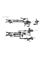
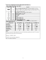
IC5202, IC5203 NT5CB256M4CN/NT5CB128M8CN - 1
Input / Output Functional description
Symbol
Type
Clock:
CK and CK are differential clock inputs. All address and control input signals
are sampled on the crossing of the positive edge of CK and negative edge of CK.
CKE
Input
Clock Enable:
CKE high activates, and CKE low deactivates,intermal clock signals
and device input buffers and output drivers. Taking CKE low provides Precharge
Power-Down and Self-Refresh operation (all banks idle), or Active Power-Down
(row Active in any bank). CKE is synchronous for power down entry and exit and for
Self-Refresh entry. CKE is asynchronous for Self-Refresh exit. After VREF has
become stable during the power on and initialization sequence, it must be maintained
for proper operation of the CKE receiver. For proper self-refresh entry and exit, VREF
must maintain to this input. CKE must be maintained high throughout read and write
accesses. Input buffers, excluding CK,CK,ODT and CKE are disabled during Power
Down. Input buffers, excluding CKE, are disabled during Self-Refresh.
Chip Select:
All commands are masked when CS is registered high. CS provides for
external rank selection on systems with multiple memory ranks. CS is considered part
of the command code.
Command Inputs: RAS,CAS and WE(along with CS) define the command being
entered.
Input Data Mask:
DM is an input mask signal for write data. Input data is masked
when DM is sampled HIGH coincident with that input data during a Write access. DM
is sampled on both edges of DQS. For x8 device, the function of DM or TDQS/TQDS
is enabled by Mode Register A11 setting in MR1.
Bank Address Inputs:
BA0, BA1 and BA2 define to which bank an Active, Read,
Input
Write or Precharge command is being applied. Bank address also determines which
mode register is to be accessed during a MRS cycle.
Address Inputs: Provide the row address for Activate commands and the column
address for Read/Write commands to select one location out of the memory array in
the respective bank. (A10/AP and A12/BC# have additional function as below. The
address inputs also provide the op-code during Mode Register Set commands.
Burst Chop:
A12/BC is sampled during Read and Write commands to determine if
burst chop (on the fly) will be performed.
(HIGH - no burst chop; LOW - burst chopped).
DQ
Input/output Data Inputs/output: Bi-dircetional data bus.
DQU,DQL
Data Strobe:
output with read data, input with write data. Edge aligned with read
DQS,(DQS)
data, centered with write data. The data strobes DQS,DQSL,DQSU are paired with
DQSL,(DQSL),
differential signals DQS, DQSL, DQSU, respectively, to provide differential pair
DQSU,(DQSU)
signaling to the system during both reads and writes, DDR3 SDRAM supports
differential data strobe only and does not support single-ended.
On Die Termination:
ODT (registered HIGH) enables termination resistance intemal
to the DDR3 SDRAM. When enabled, ODT is applied to each DQ, DQS, DQS# and
DM/TDQS, NU/TDQS# (when TDQS is enabled via Mode Register A11=1 in MR1)
signal for x8 configuratlons. The ODT pin will be ignored if MR1 and MR2 ard
programmed to disable RTT.
Active Low Asynchronous Reset:
Reset is avtive when RESET# is LOW, and
inactive when RESET# is HIGH. RESET# must be HIGH during normal operation.
RESET# is a CMOS rail to rail signal wigh DC high and low at 80% and 20% of VDD,
I,e, 1.20V for DC high and 0.30V.
CK,CK
BA0 - BA2
DM,(DMU,DML)
ODT
Function
Input
Input
A0 - A13
Input
Input/output
RESET
Input
Input
Input
CS
RAS,CAS,WE
Input
A12 / BC#
Input
Summary of Contents for BDX2500KU
Page 10: ...3 5 Audio Output Circuit Diagram IC9001 TK11150CSCL G AK4424AET E2 IC9002 ...
Page 11: ...3 6 Video Output Circuit Diagram IC4001 BCM7630BKFEBG Video DAC ...
Page 12: ...3 7 HDMI Output Circuit Diagram IC4001 BCM7630BKFEBG IC2301 TK11150CSCL GH HDMI ...
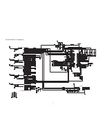
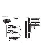
Page 16: ...DDR3 Circuit Diagram 3 11 DDR3 IC4001 BCM7630BKFEBG ...
Page 19: ...Motor Servo Connect Circuit Diagram 3 14 IC4501 LD1117SC R ...
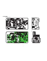
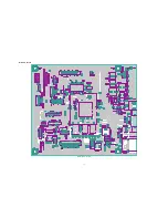
Page 23: ...4 3 Main PC Board Main PC Board Top Side ...
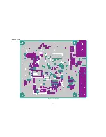
Page 24: ...4 4 Main PC Board Main PC Board Bottom Side ...
Page 37: ...7 1 EXPLODED VIEW 1 2 3 7 4 6 8 9 5 ...
Page 52: ...1 1 SHIBAURA 1 CHOME MINATO KU TOKYO 105 8001 JAPAN ...

