background image

- 3 -

GENERAL

ADJUSTMENTS

SPECIFIC

INFORMATIONS

 SERVICE SAFETY PRECAUTIONS

• The caution items shown here describe major safety issues and should always be observed.
• The meanings of the various indications are as follows.

WARNING

 CAUTION

Indicates a hypothetical situation in which service personnel and nearby third parties, or even
end users due to a product defect after the service operation is completed, could possibly be in
danger of injury or even death in the event of operational error.

Indicates a hypothetical situation in which service personnel and nearby third parties, or even
end users after the service operation is completed, could possibly be in danger of injury, or
where there could be physical damage in the event of operational error.

* Physical damage means major damage to a home, furnishings and other possessions.

Examples of marks

SHOCK HAZARD

PROHIBIT DISASSEM-

BLING

UNPULUG

The

"

 indicates caution (including danger and warning).

The actual meaning of this caution is indicated inside the 

"

 or nearby illustrations or text.

The example shown to the left indicates the danger of "electrical shock".

The

 indicates a forbidden action.

The actual meaning of this caution is indicated inside the   or nearby illustrations or text.
The example shown to the left indicates that disassembly is forbidden.

The

-

 indicates  a forced action (an action that must be performed).

The actual meaning of this forced action is indicated by 

-

 or nearby illustrations or text.

The example shown to the left indicates that the power plug must be disconnected.

Summary of Contents for 27HLV95

Page 1: ... 1 SERVICE MANUAL LCD Color Television 27HLV95 FILE NO 020 200515 Published in Japan Jul 2005 YC TOSHIBA CORPORATION 2005 ...

Page 2: ...LING THE LCD MODULE 5 SERVICE MODE 7 LAYOUT OF MAJOR BOARDS 12 MECHANICAL DISASSEMBLY 13 EXPLODED VIEW 15 PACKING DISASSEMBLY 17 CHASSIS AND CABINET REPLACEMENT PARTS LIST 18 PC BOARDS TOP BOTTOM VIEW 25 CIRCUIT BLOCK DIAGRAM 51 APPENDIX SCHEMATIC DIAGRAM ...

Page 3: ...f injury or where there could be physical damage in the event of operational error Physical damage means major damage to a home furnishings and other possessions Examples of marks SHOCK HAZARD PROHIBIT DISASSEM BLING UNPULUG The indicates caution including danger and warning The actual meaning of this caution is indicated inside the or nearby illustrations or text The example shown to the left ind...

Page 4: ...ark is included in a circuit diagram or parts list Parts mounting and routing of the wiring should be the same as that used originally For safety purposes insulating materials such as tubing or tape is sometimes used and printed circuit boards are sometimes mounted floating Also make sure that wiring is routed and clamped to avoid parts that generate heat and which use high voltage Always follow t...

Page 5: ...of the LCD module with the corresponding holes in the LCD cover and fasten with screws Do not strongly push on the mod ule because any impact can adversely affect the perform ance Also use caution when handling the polarized screen because it can easily be damaged CAUTION The metal edges of the LCD module are sharp so use caution to avoid in jury 3 If the panel surface becomes soiled wipe with cot...

Page 6: ... loss of resilience or other damage 9 Do not disassemble the LCD module Such actions could result in improper operation 10 When transporting the LCD module do not use packing containing epoxy resin amine or silicon resin alcohol or oxim The gas generated by these materials can cause loss of polarity Safety Precautions for Laser Beam DVD Player Do not look into the opening of the disc slot or venti...

Page 7: ...E Test signal selection TV VIDEO button on Remote Selection of the adjustment items Channel on TV or Remote Change of the data value Volume W X on TV or on Remote Adjustment menu mode ON OFF MENU button on Remote Initialization of the memory CALL Channel button on TV Reset the count of operating protect circuit to 00 CALL Channel button on TV RCUT selection 1 button GCUT selection 2 button BCUT se...

Page 8: ...R button to turn off the TV once INITIALIZATION OF MEMORY DATA After replacing EEPROM IC the following initialization is required 1 Enter the service mode then select any register item 2 Press and hold the CALL button on the Remote then press the CHANNEL button on the TV The initialization of EEPROM IC has been completed 3 Check the picture carefully If necessary adjust any adjustment item above P...

Page 9: ...icroprocessor In case of file name HLV95 and Version 1489 indicates HLV95_1489 2 Time Total hour of turn the TV on Unit H 3 Bus line OK is normal SCL GND Red indication SCL GND short circuit SDA GND Red indication SDA GND short circuit SCL SDA Red indication SCL SDA short circuit 4 Bus cont OK is normal NG is abnormal Red indication When type name of semiconductor indicates 5 Block UV TV reception...

Page 10: ...sion 1489 for Code Program Version and U15 for OSD Version indicates HLV95_1489 U15 2 EEPROM Version information of EEPROM Display 1 byte data 3 SUB MPU Version information of SUB MPU Display 1 byte data 4 OPTION Option information Display six numbers of 1 byte data 5 HDMI ID HDMI ID information Display 4 byte data 6 DVD DVD information Display 1 byte data 7 LCD Panel Vender information display Th...

Page 11: ...isplay RF position number 0 99 on the main screen or Input Source ANT1 2 HDMI etc 2 MAIN FORMAT Display Video and PC format information 3 MAIN PLL Main PLL information Display five numbers of 2 byte data 4 SCREEN SIZE Display the screen size as follows ANT1 CABLE 12 480i NATURAL 06 OF B0 CE 02 0000 0000 0000 1 2 4 5 3 5 OTHER STATUS Other status information Display three numbers of 2 byte data The...

Page 12: ...S U105A TN AV AOUT BOARD U101 SIGNAL DVD LCD BOARD U104 RF SW TIF BOARD U105C KEY SW BOARD U105B LED RMT BOARD U105E DVD KEY BOARD U802 AC IN BOARD U105D PC IN BOARD U102 SEINE FOR FPD BOARD U103 D TUNER BOARD U801 POWER BOARD ...

Page 13: ...W W SBN 2 PP4 12 SW W SBN 2 BITTB3 12 SBN 2 PP4 12 SW W SBN PP3 8 SW W SBN PP3 8 SW W SBN PP3 8 SW W SBN PP4 12 SW W SBN 6 PP3 8 SW W ECO 3 PP3 8 SW W ECO 3 PP4 12 SW W SBN 2 BITTB3 8 ECO 2 A340 A507 BD01 A525 A320 U105C H003C U105D 4 40UNC JFS 4S L 13 2 BITTB3 8 ECO 4 PP3 8 SW W SBN 2 PP3 8 SW W SBN 2 PP3 8 SW W SBN 4 PP3 8 SW W SBN 4 PP3 8 SW W SBN PP3 8 SW W SBN BITTB3 8 ECO 3 BITTB3 12 SBN 2 U...

Page 14: ...SW W ECO 4 PP4 20 SW W SBN 2 PP3 8 SW W ECO 5 PP3 8 SW W ECO 3 PP3 8 SW W ECO 4 U105B U105A U801 U802 U101 U103 U102 3 Remove the boards SIGNAL DVD LCD SEINE FOR FPD D TUNER TN AV AOUT LED RMT POWER AC IN and speaker 4 Remove the display W661 W661 BITTB4 16 SBN 4 BITTB4 16 SBN 4 PP08 PP08 B001 A201 PP4 12 SW W SBN 4 BITTB4 16 SBN 14 ...

Page 15: ...W SBN PP3 8 SW W SBN PP3 8 SW W SBN 2 PP3 8 SW W SBN 2 PP3 8 SW W SBN 4 PP3 8 SW W SBN 4 PP3 8 SW W SBN PP3 8 SW W SBN PP3 8 SW W SBN PP4 12 SW W SBN 6 BITTB3 12 SBN 2 BITTB3 8 ECO 3 BITTB3 12 SBN 2 PP4 12 SW W SBN 2 BITTB3 12 SBN 10 PP3 8 SW W SBN 4 A450 A445 A401 A420 PP5 16 SW W SBN 5 A340 BD01 A525 A501 A320 U105C U105E U105D U104 H003C PP3 8 SW W ECO 3 PP3 8 SW W ECO 3 ...

Page 16: ...P3 8 SW W ECO 6 BITTB4 16 SBN 4 BITTB4 16 SBN 4 PP3 8 SW W ECO 5 PP3 8 SW W ECO 4 PP3 8 SW W ECO 5 BITTB3 8 ECO 2 PP4 12 SW W SBN 4 BITTB4 16 SBN 14 PP08 PP08 PP08 UF03 PP08 PP08 PP08 W661 W661 A201 B001 PP3 8 SW W SBN 2 P801 A315 U105B U105A U801 U802 U101 U103 U102 2 Main Block ...

Page 17: ... 17 PACKING DISASSEMBLY A702B A702B A702A A702A Y170 Y101 A701A A703 K902 ...

Page 18: ...AMIC CHIP 16V B 1UF K C678 76285104 CERAMIC CHIP 50V B 0 1UF K C679 76285104 CERAMIC CHIP 50V B 0 1UF K C680 76073073 ELECTROLYTIC 35V 2200UF M 3A C681 76073073 ELECTROLYTIC 35V 2200UF M 3A C682 76073073 ELECTROLYTIC 35V 2200UF M 3A C684 76109103 CERAMIC CHIP 50V B 0 01UF K C685 76619113 ELECTROLYTIC CHIP 50V 1UF M C690 76669101 ELECTROLYTIC 50V 100UF M C691 76092463 CERAMIC CHIP 16V B 0 22UF K C6...

Page 19: ...TROLYTIC 16V 100UF M CE94 76503047 PLASTIC FILM 63V 0 33UF J CE95 76503041 PLASTIC FILM 63V 0 1UF J CE96 76794101 ELECTROLYTIC 16V 100UF M CS10 76092628 CERAMIC CHIP 6 3V B 10UF K CS11 76092628 CERAMIC CHIP 6 3V B 10UF K CS12 76109473 CERAMIC CHIP 25V B 0 047UF K CS15 76092628 CERAMIC CHIP 6 3V B 10UF K CS16 76092628 CERAMIC CHIP 6 3V B 10UF K CS40 76092611 CERAMIC CHIP 6 3V B 2 2UF K CS41 7609261...

Page 20: ...D12 76011152 CHIP 1 20W 1 5K OHM J RD21 76367101 CARBON FILM 1 6W 100 OHM G RD22 76367222 CARBON FILM 1 6W 2 2K OHM G RD31 76011153 CHIP 1 2OW 15K OHM J RD32 76011473 CHIP 1 20W 47K OHM J RD41 76011101 CHIP 1 20W 100 OHM J RD43 76000445 CHIP JUMPER 1608TYPE RD44 76000445 CHIP JUMPER 1608TYPE RD45 76011101 CHIP 1 20W 100 OHM J RD50 76000445 CHIP JUMPER 1608TYPE RD51 76000445 CHIP JUMPER 1608TYPE RD...

Page 21: ...011182 CHIP 1 20W 1 8K OHM J RS66 76011100 CHIP 1 20W 10 OHM J RS78 76011102 CHIP 1 20W 1K OHM J RS81 76011102 CHIP 1 20W 1K OHM J RS82 76011682 CHIP 1 20W 6 8K OHM J RS87 76011101 CHIP 1 20W 100 OHM J RS88 76011101 CHIP 1 20W 100 OHM J RS500 76011103 CHIP 1 20W 10K OHM J RS501 76011153 CHIP 1 2OW 15K OHM J RS504 76011153 CHIP 1 2OW 15K OHM J RS505 76011103 CHIP 1 20W 10K OHM J RS516 76011101 CHIP...

Page 22: ...809API U P QE92 23205446 TRANSISTOR 2SC2412K Q T146 QE93 23205301 TRANSISTOR 2SA1887 FA F QE94 23205292 TRANSISTOR 2SD2396 QE95 23205446 TRANSISTOR 2SC2412K Q T146 QE96 23205301 TRANSISTOR 2SA1887 FA F QE97 23205569 TRANSISTOR CHIPVCEO 120V2SC2713 GR TE85L F QE98 23205568 TRANSISTOR CHIPVCEO 120V2SA1163 GR TE85L F QS01 23009916 IC MM1631AJBE QS03 23205302 TRANSISTOR 2SC3326 B F QS04 23205302 TRANS...

Page 23: ...DUNITIR CTVUSACT 90236 KB01 23009710 REMOCONRECEIVER GP1UE281RK MJ22 23389359 CABLE FFC 0 5 50P L70 GOLD MJ60 23389359 CABLE FFC 0 5 50P L70 GOLD MV97 23389344 FFC 20706SFWR P 1 0 L1 13 223P1 0 13P 230B WR MZ01 23513230 CABLE LVDS30P250MM COM T4 E30 S30 P601 23713755 PLUG 4P 2 5MM G B4B EH F1 TV4 P602A 23713937 CONNECTOR PLUG4PB4B PH K S LF P602B 23713937 CONNECTOR PLUG4PB4B PH K S LF P661 2302330...

Page 24: ...N TUNER H001 23321536 TUNER TIF US HOR IIC PH 864M ENG36A36GF ACCESSORIES A701A 23015147 CARTON CASE27HLV95 A702A 23946986 PACKING TOP PACKING A702B 23946987 PACKING BOTTOMPACKING A703 23945190 BAG PROTECTIVE K903 23306630 REMOCONHANDUNIT CT 90236 Y101 23566697 OWNERSMANUAL ENG FRE SPA27HLV95 Y170 23845800 HOLDER WIRE NYLON66 D6 8 CABINET PARTS A201 23533519 COVER FRONT BEZEL ASSY A231 23717214 SC...

Page 25: ...SIGNAL DVD LCD BOARD PD2222A1 U101 BOTTOM FOIL SIDE 25 26 ...

Page 26: ...SIGNAL DVD LCD BOARD PD2222A1 U101 TOP COMPONENT SIDE 27 28 ...

Page 27: ...SEINE FOR FPD BOARD PD2266F1 U102 BOTTOM FOIL SIDE 29 30 ...

Page 28: ...SEINE FOR FPD BOARD PD2266F1 U102 TOP COMPONENT SIDE 31 32 ...

Page 29: ...D TUNER BOARD PD2232A1 U103 BOTTOM FOIL SIDE D TUNER BOARD PD2232A1 U103 TOP COMPONENT SIDE 33 34 ...

Page 30: ...0 C164 GR04 GR112 R167 L190 C114 C153 R151 C152 L152 L151 R152 C151 H001 GR114 PJ23B GR01 L102 PK05 GR05 L110 L105 GR02 GR03 C190 R113 GR113 C119 R103 C107 R165 R104 L103 R107 L101 C105 Q161 D101 R115 R161 C117 C113 C103 C161 C109 GR612 C101 Q102 R110 R108 C116 C162 R114 C102 R166 Q101 C118 C111 R105 R168 R112 GR613 C115 R111 C112 C104 C110 C164 GR04 GR112 R167 L190 C114 H003 C153 R151 C152 L152 L...

Page 31: ...7 R681 Q664 C661 R680 C663 C684 C664 R664 D676 R6606 C668 Q660 C662 Q661 R670 RE95 R6604 Q670 R675 R6602 C670 D680 C665 Q663 QS03 R690 D681 C692 C674 R677 RS81 CS11 RS78 C669 Q672 R674 R672 P803B Q665 D679 DE93 R6601 R671 D670 R6603 C678 DE94 R673 RS20 Q671 C671 C666 CS10 R683 C691 R676 QS04 CV61 RV44 RV43 RV42 RV41 RS58 RS59 GJ002 CV26 CV25 LV33 CS80 LV31 CS53 RS66 RS19 RS55 RV62 CV58 GR07 RS40 R...

Page 32: ...0 LV287 RD82 RD81 CS54 RV203 CD88 GJ413 RD86 CD83 LD01 PJ22A R4109 Q4109 C168 CD85 RD90 RD89 CS82 CD87 RS44 RS88 RV200 R4121 RV205 CD91 RD85 RS82 QS01 CD95 DD81 CS64 RS54 R4103 R4120 CS503 R4104 Q4101 C667 C681 RS504 RS507 C660 RS506 CE87 C661 GRS02 RS505 C673 C664 C169 C670 C665 CS504 CS501 Q670A PJ60A RS516 RS517 P803B RS500 CS505 P602A QS102 CS502 C671 C685 C666 Q4108 CE91 FE94 DE89 CE96 RE97 Q...

Page 33: ... SA04 SA08 RA71 RA77 DA15 DA11 DA13 DA12 SA03 RA74 SA02 RA79 RA78 RA73 SA07 SA01 RA72 PJ42 DA14 RA76 RA71 RA77 DA14 DA15 DA11 DA13 DA12 RA74 RA79 RA78 RA73 RA72 13 12 11 10 9 8 7 6 5 4 3 2 1 4 PD2217 23590300 PV90 PV97A PS15 KEY SW BOARD PD2217A3 U105C BOTTOM FOIL SIDE KEY SW BOARD PD2217A3 U105C TOP COMPONENT SIDE 8 7 6 5 4 3 2 1 PD2217 CH UP CH DN VOL UP POWER 23590300 3 4 3 2 1 VOL DN VIDEO TEX...

Page 34: ...D76 SA15 SA14 RD74 SA12 SA11 RD78 PJ43 RD73 RD77 RD76 RD74 RD78 2 1 4 3 5 PD2217 23590300 PLAY STOP SKIP FWD SKIP REV EJECT PJ43 SA13 SA15 SA14 SA12 SA11 DVD KEY BOARD PD2217A5 U105E BOTTOM FOIL SIDE DVD KEY BOARD PD2217A5 U105E TOP COMPONENT SIDE ...

Page 35: ...D2237 1 C888 R862 DE73A DE51 L889 L883 R861 LE53 L888 LE73 QE73 P813B P803A P805 P804 PJ80A QE75 D884 QE92 CE51 GJ82 GJ84 QE52 RE57 RE92 RE53 DE50 LE74 RE73 GJ841 CE54 RE52 CE73 RE74 DE52 D883 CE76 RE60 CE43 CE52 QE93 L890 GJ889 D884A CE50 C883 QE93A RE78 CE53 RE83 CE75 RE56 CE74 QE83 RE82 RE43 CE55 RE55 RE58 RE79 LE72 RE61 QE40 RE49 FE76 RE45 LE71 QE53 DE54 DE73 DE56 CE83 CE41 RE46 GE51 RE54 D885...

Page 36: ...2 5 4 3 2 4 3 2 1 4 3 2 1 P800 D899 P805B R801 T801 GAP C801 R899 L802 C812 CE13 DE02 DE03 RE 03 LE07 P812A L801 GJ94 CE02 C811 F801B RE04 CE14 F801 C802 GJ90 F801A GJ89 GJ88 T802 GJ87 C80 5 CE04 P813A C8100 C8110 C E 0 5 LE06 C 8 0 6 L806 L807 P811A GJ92 GJ91 C851 D801 SR81 GJ93 R828 R853 Q854 D852 R857 Q851 R854 R856 C852 R859 Q853 Q852 R852 R858 R850 R855 D801A R827 Q855 DE01 R851 C851 R853 Q85...

Page 37: ... indicated to chassing ground using a color bar signal with all controls at normal line voltage 220 volts 5 Waveforms are taken receiving color bar signal with enough sensitivity 6 Voltage reading shown are nominal values and may vary 20 except H V MODEL 27HLV95 SCHEMATIC DIAGRAM WARNING BEFORE SERVICING THIS CHASSIS READ THE SERVICE SAFETY PRECAUTIONS ON PAGE 3 OF THIS MANUAL CAUTION The internat...

Page 38: ...ET 309 28 129 EEPROM2 SHEET 310 29 129 MICRO I O SHEET 400 30 129 OCM MEMORY I F SHEET 401 31 129 FLASH MEMORY SHEET 402 32 129 SYNC SEPA SHEET 403 33 129 E2P OTHER SHEET 404 34 129 STD BY MICOR SHEET 405 35 129 CORTEZ REG 1 SHEET 406 36 129 CORTEZ REG 2 SHEET 407 37 129 CORTEZ REG 3 SHEET 408 38 129 BOOT CONFIG SHEET 409 39 129 SERVICE CONNECTOR SHEET 410 40 129 I2C Switch SHEET 411 41 129 STBY M...

Page 39: ... 81 129 VIDEO POWER SHEET 210 82 129 SEINE DIGITAL OUT SHEET 220 83 129 SEINE BEP IF SHEET 221 84 129 SEINE DAC OUT SHEET 225 85 129 DOWN CON OUT DRIVER SHEET 226 86 129 HD OUT LPF SHEET 227 87 129 MACRO VCD 1 2 SHEET 240 88 129 2 2 SHEET 241 89 129 VIDEO LPF SHEET 242 90 129 MPEG Enc CLK SDRAM SHEET 250 91 129 MPEG Enc AV I F SHEET 251 92 129 MPEG Enc STREAM I F SHEET 252 93 129 MPEG Enc POWER SH...

Page 40: ...17 129 DDR 3 SHEET 904 118 129 DDR 4 SHEET 905 119 129 DDR POWER SHEET 906 120 129 TERMINATOR SHEET 907 121 129 VCXO SHEET 941 122 129 SEINE VDD VSS SHEET 950 123 129 SIGNAL CONNECTOR SHEET 960 124 129 POWER CONNECTOR SHEET 961 125 129 Signal filter SHEET 964 126 129 D TUNER TUNER CONNECTOR TUNER SHEET 104 127 129 OOB FDC SHEET 105 128 129 FAT TUNER SHEET 106 129 129 ...

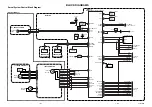
Page 41: ... Enc Audio ADC Digital Tuner POD AudioDAC Y Cb Cr D Composite Analog Tuner V2 MONI OUT REC OUT HDMI_1 HDMI_2 V1 S1 MONI SW DVD Built in unit Y Pb Pr PC in R G B HD VD CS1 CS2 CS SW Y Pb Pr_2 2Vpp TV1 Y Pb Pr_1 Analog Front End Video Decoder MUX VBI Data Processor DCDi MADi Scaling LVDS Micro processor IR I F ADC GPIO Digital Input A Digital Input B 2nd Channel Process 1Vpp TV or E1 6dB BEP VIDEO R...

Page 42: ......

Reviews: