background image

ELECTRICAL ADJUSTMENTS

D-2

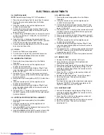
2-11: BRIGHT CENT

1.
2.

3.
4.

5.

6
7.

Receive the PAL black pattern*. (RF Input)
Using the remote control, set the brightness and
contrast to normal position.
Place the set with Aging Test for more than 15 minutes.
Activate the adjustment mode display of Fig. 1-1 and
press the channel button (17) on the remote control to
select "BRIGHT CENT".
Press the VOL. +/- button on the remote control until
the screen begin to shine.
Receive the PAL black pattern*. (Audio Video Input)
Set to the AV mode. Then perform the above
adjustments 2~5.

*The Black Pattern means the whole black raster signal.

Select the "RASTER" of the pattern generator, set to
the OFF position for each R, G and B.

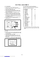
2-12: CONTRAST CENT

1.

2.

3.
4.

Activate the adjustment mode display of Fig. 1-1 and
press the channel button (22) on the remote control to
select "CONTRAST CENT".
Press the VOL. +/- button on the remote control until
the contrast step No. becomes "35".
Receive a broadcast and check if the picture is normal.
Set to the AV mode. Then perform the above
adjustments 1~3.

Receive an 70dB monoscope pattern.
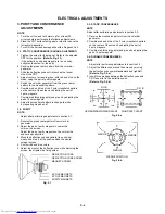
Turn the Focus Volume fully counterclockwise once.
Adjust the Focus Volume until picture is distinct.

2-7: FOCUS

1.
2.
3.

2-8: HORIZONTAL POSITION

1.

2.

3.

4.

5.

6.

7.

8.

Receive the monoscope pattern from the Pattern
Generator.
Using the remote control, set the brightness and
contrast to normal position.
Activate the adjustment mode display of Fig. 1-1 and
press the channel button (08) on the remote control to
select "H POSI (50)".
Press the VOL. +/- button on the remote control until
the SHIFT quantity of the OVER SCAN on right and left
becomes minimum.
Receive the monoscope pattern of NTSC. (Audio Video
Input)
Using the remote control, set the brightness and
contrast to normal position.
Activate the adjustment mode display of Fig. 1-1 and
press the channel button (39) on the remote control to
select "H POSI (60)".
Press the VOL. +/- button on the remote control until
the SHIFT quantity of the OVER SCAN on right and left
becomes minimum.

Receive the monoscope pattern from the Pattern
Generator.
Using the remote control, set the brightness and
contrast to normal position.
Activate the adjustment mode display of Fig. 1-1 and
press the channel button (11) on the remote control to
select "V SIZE (50)".
Press the the VOL. +/- button on the remote control until
the SHIFT quantity of the OVER SCAN on upside and
downside becomes 8 

±

 2%.

Receive a broadcast and check if the picture is normal.
Receive the monoscope pattern of NTSC. (Audio Video
Input)
Using the remote control, set the brightness and
contrast to normal position.
Activate the adjustment mode display of Fig. 1-1 and
press the channel button (12) on the remote control to
select "V SIZE (60)".
Press the the VOL. +/- button on the remote control until
the SHIFT quantity of the OVER SCAN on upside and
downside becomes 10 

±

 2%.

Receive a broadcast and check if the picture is normal.

2-10: VERTICAL SIZE

1.

2.

3.

4.

5.
6.

7.

8.

9.

10.

2-9: VERTICAL POSITION, VERTICAL LINEARITY

1.

2.

3.

4.

Receive the monoscope pattern from the pattern
Generator.
Using the remote control, set the brightness and
contrast to normal position.
Adjust the VR401 until the horizontal line becomes fit to
the notch of the shadow mask.
Adjust the VR420 until the SHIFT quantity of the OVER
SCAN on upside and downside becomes minimum.

2-6: WHITE BALANCE

NOTE: Adjust after performing CUT OFF adjustment.

1.
2.

3.

4.

5.

6.

7.

Place the set with Aging Test for more than 15 minutes.
Receive the gray scale pattern from the Pattern
Generator.
Using the remote control, set the brightness and
contrast to normal position.
Activate the adjustment mode display of Fig. 1-1 and
press the channel button (03) on the remote control to
select "R DRIVE".
Press the Page UP/DOWN button on the remote control
to select the "R DRIVE", "G DRIVE", "M R CUTOFF" or
"M G CUTOFF".
Adjust the VOL. +/- button on the remote control to
whiten the R DRIVE, G DRIVE, M R CUT OFF, and M G
CUT OFF at each step tone sections equally.
Perform the above adjustments 5 and 6 until the white
color is looked like a white.

Summary of Contents for 21N21F

Page 1: ...SERVICE MANUAL PRINTED IN UK 2002 C COLOURTELEVISION 21N21F TOSHIBA ...

Page 2: ...which has the same character Especially as to the important parts for safety which is indicated in the circuit diagram or the table of parts as a mark the designated parts must be used 4 PUT PARTS AND WIRES IN THE ORIGINAL POSITION AFTER ASSEMBLING OR WIRING There are parts which use the insulation material such as a tube or tape for safety or which are assembled in the condition that these do not...

Page 3: ...WHEN REPLACING EEPROM MEMORY IC ELECTRICAL ADJUSTMENTS BLOCK DIAGRAM PRINTED CIRCUIT BOARDS MAIN CRT SCHEMATIC DIAGRAMS MICON TUNER IF CHROMA 21PIN AV SW DEFLECTION CRT POWER SOUND AMP WAVEFORMS MECHANICAL EXPLODED VIEW MECHANICAL REPLACEMENT PARTS LIST ELECTRICAL REPLACEMENT PARTS LIST A1 1 A1 1 A1 1 A2 1 A3 1 A3 5 B1 1 B2 1 B2 2 C 1 C 1 C 2 D 1 D 5 E 1 E 2 F 1 F 4 G 1 G 2 G 3 G 4 G 5 G 6 G 7 G 8...

Page 4: ...F UHF 75 ohm CH Coverage E2 E4 X Z 2 S1 S10 E5 E12 S11 S41 E21 E69 Intermediate PAL SECAM U VH SECAM VL Frequency Picture FP 38 9 38 9 34 4MHz Sound FS 33 4 32 4 40 9MHz FP FS 5 5 6 5 6 5MHZ PAL DK SECAM DK Picture FP 38 9 38 9 MHz Sound FS 32 4 32 4 MHz FP FS 6 5 6 5MHz Auto Tuning Method ALL Band Not C C I R CH Plan Preset CH 100 Stereo Dual TV Sound No Tuner Sound Muting Yes G 3 Power Power Sou...

Page 5: ...ock Yes Nicam Auto Off No AV Color System Yes Sound System No Auto 4 3 Default No AV2 Output No Output Source No Source No Control Level Yes Volume Yes Brightness Yes Contrast Yes Color Yes Tint NTSC Only Yes Sharpness Yes Tuning Yes Bass No Treble No Balance No Back Light No Nicam ST No Tone 1 2 A B No Surround On Off No Pin Code No AV Yes Skip Yes Channel Yes Hotel Lock No Sleep Timer No Selecta...

Page 6: ...wer Source Voltage D C 3V UM size x pcs UM 4 x 2 pcs Total Keys 32 Keys Keys Power Yes 1 Yes 2 Yes 3 Yes 4 Yes 5 Yes 6 Yes 7 Yes 8 Yes 9 Yes 0 Yes Volume Up Yes Volume Down Yes Previous Yes Select Picture Yes Menu Yes OK Enter Yes EXIT No Audio Select No Sleep Timer No Mute Yes T TEXT Keys TEXT MIX TV Yes CH Up Page Up Yes CH Down Page Down Yes Red Yes Green Yes Yellow Yes Cyan Yes TEXT F T B Yes ...

Page 7: ...ble Focus Dynamic Focus No Wss Signal Wide Change No Virtual Dolby Surround No Hotel Lock No G 12 Accessories Owner s Manual Language French Germany Polish Hungarian Czech w Guarantee Card No Remote Control Unit Yes Rod Antenna No Poles Pole Terminal type Loop Antenna No Terminal U V Mixer No DC Car Cord Center No Guarantee Card No Warning Sheet No Circuit Diagram No Antenna Change Plug No Service...

Page 8: ...ro Scart 21Pin Yes x1 RGB INPUT Yes x1 Component Input No Diversity No Ext Speaker No DC Jack 12V Center No VHF UHF Antenna Input D Type AC Outlet No G 14 Set Size Approx W x D x H mm 506 6 x 484 x 464 5 G 15 Weight Net Approx 21 0 kg lbs Gross Approx 23 8kg lbs G 16 Carton Master Carton No Content Sets Material Dimensions W x D x H mm x x Description of Origin Gift Box Yes Material Double Brown D...

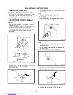
Page 9: ...ip up the sides of the Rubber Cap in the direction of the arrow and remove one side of the support Refer to Fig 1 2 2 DISASSEMBLY INSTRUCTIONS GND on the CRT Screwdriver Alligator Clip Support CRT GND on the CRT Rubber Cap CRT Support Fig 1 1 Fig 1 2 3 After one side is removed pull in the opposite direction to remove the other NOTE Take care not to damage the Rubber Cap INSTALLATION 1 Clean the s...

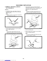
Page 10: ...using a blower type IC desoldering machine Refer to Fig 2 2 2 Fig 2 2 NOTE Do not add the rotating and the back and forth directions force on the IC until IC can move back and forth easily after desoldering the IC leads completely When IC starts moving back and forth easily after desoldering completely pickup the corner of the IC using a tweezers and remove the IC by moving with the IC desoldering...

Page 11: ...2 8 Thin tip Soldering Iron NOTE When the IC leads are bent during soldering and or repairing do not repair the bending of leads If the bending of leads are repaired the pattern may be damaged So be always sure to replace the IC in this case Finally confirm the soldering status on four sides of the IC using a magnifying glass Confirm that no abnormality is found on the soldering position and insta...

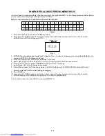
Page 12: ...conds After the confirmation of using hours turn off the power ADDRESS DATA INIT 01 00 CRT ON 0010 FIG 1 Initial setting content of MEMORY IC POWER ON total hours 16 x 16 x 16 x thousands digit value 16 x 16 x hundreds digit value 16 x tens digit value ones digit value VOL MIN 1 Initialization of the factory NOTE Do not use this for the normal servicing If you set a factory initialization the memo...

Page 13: ...ep through the ADDRESS until required ADDRESS to be changed is reached Press OK to select DATA When DATA is selected it will blink Again step through the DATA using VOL button until required DATA value has been selected Pressing OK will take you back to ADDRESS for further selection if necessary Repeat steps 3 to 6 until all data has been checked When satisfied correct DATA has been entered turn P...

Page 14: ...on on the remote control to select the options shown in Fig 1 2 Press the MENU button on the remote control to end the adjustments NO 20 21 22 23 24 25 26 27 28 29 30 31 32 33 34 35 36 37 38 39 FUNCTION CUT OFF RF AGC AGC GAIN R DRIVE R CUTOFF G DRIVE G CUTOFF B DRIVE H POSI 50 V POSI 50 V POSI 60 V SIZE 50 V SIZE 60 VCO COARSE VCO FINE VCO COARSE L1 VCO FINE L1 BRIGHT CENT BRIGHT MAX BRIGHT MIN N...

Page 15: ...control until the SHIFT quantity of the OVER SCAN on right and left becomes minimum Receive the monoscope pattern from the Pattern Generator Using the remote control set the brightness and contrast to normal position Activate the adjustment mode display of Fig 1 1 and press the channel button 11 on the remote control to select V SIZE 50 Press the the VOL button on the remote control until the SHIF...

Page 16: ...ast and color to normal position Connect the oscilloscope to TP801 Activate the adjustment mode display of Fig 1 1 and press the channel button 25 on the remote control to select COLOR CENT Adjust the VOLTS RANGE VARIABLE knob of the oscilloscope until the range between white 100 and 0 is set to 5 scales on the screen of the oscilloscope Press the VOL button on the remote control until the red col...

Page 17: ...Switch the color bar generator from the green raster pattern to the crosshatch pattern Combine red and blue of the 3 color crosshatch pattern on the center of the screen by adjusting the pair of 4 pole magnets Combine red blue magenta and green by adjusting the pair of 6 pole magnets Adjust the crosshatch pattern to change to white by repeating steps 6 and 7 Turn the unit on and let it warm up for...

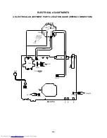
Page 18: ...CATION GUIDE WIRING CONNECTION D 5 CP803B CP802B CP801 CRT J801 FB401 CP101 TU001 J702 J704 J703 CP803A CP802A TP801 TP803 CRT CP401 CP501 AC IN CD501 SPEAKER CP1002 CP502 CRT VR501 TP501 R521 MAIN PCB CRT PCB CD803 CD802 L503 TP001 VR420 VR401 C D 801 J701 ...

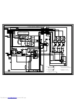
Page 19: ...N 25V Q805 Q806 BULE OUT Q803 Q804 GREEN OUT Q801 Q802 RED OUT J801 6 11 8 F 7 Q402 H DRIVE Q401 H OUTPUT I2C DY 1 F S 2 3 HV B P CON 25V CRT V801 8 3 3 4 2 6 7 5 1 HEADPHONE JACK J702 SPEAKER SP353 5 12 9 SOUND B 15 B P CON 8V D Q501 POWER 56 KEY_IN CH DOWN CH UP VIDEO_SW IC702 NJM2234L V OUT SW1 2 7 SW2 4 CVBSIN2 20 AV1 42 AV2 43 J701 3 1 VIN1 1 2 6 8 19 20 INT_CVBS_OUT 13 VIDEO OUT VIDEO IN R O...

Page 20: ...7 C528 C533 Q511 C511 C523 Q505 D506 R514 TH501 CP502 D517 C522 R507 D406 W054 D404 R410 R431 D514 D521 D527 R548 W055 R445 W056 W057 R532 VR501 W059 D604 W060 W061 W062 R542 T501_1 W063 W065 W066 W067 W069 TP501 W825 L715 W071 W072 W073 W074 W075 W076 B702 B701 C1002 C1012 W077 D101 D103 W078 C408 C130 L202 R503 X602 W080 W081 W833 W082 W083 B504 W086 D508 D407 R409 C757 W090 C540 W093 W095 W096 ...

Page 21: ...9 C731 C727 R718 R723 R724 R736 R737 C716 C721 C719 R705 R710 C712 Q602 Q603 Q711 Q601 R217 C603 C607 R142 R141 R140 R143 Q503 R502 R133 R005 R137 SH501 R412 R408 R420 R523 R535 R531 C541 R516 R510 C513 R518 R519 C502 R538 Q510 Q512 Q508 R537 R614 C629 C612 C638 C605 R129 R128 C139 C007 C543 R534 R152 C140 R151 R108 R541 C633 R107 R745 C530 C759 R1016 R1017 C1016 C211 R720 R406 R632 R1015 C105 W85...

Page 22: ...ED010 VOL DOWN SW102 SKHVBED010 CH UP SW104 SKHVBED010 CH DOWN SW106 SKHVBED010 VOL UP OF PRINTING AND SUBJECT TO CHANGE WITHOUT NOTICE NOTE THIS SCHEMATIC DIAGRAM IS THE LATEST AT THE TIME WAS RECEIVED IN GOOD CONDITION AND PICTURE IS NORMAL WITH THE DIGITAL TESTER WHEN THE COLOR BROADCAST NOTE THE DC VOLTAGE AT EACH PART WAS MEASURED Vout B GND OS101 RPM7138 H5 1 2 3 TM101 R25 1800 BT102 R03 AB ...

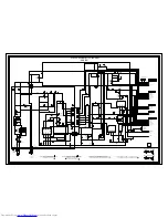
Page 23: ...26 0 1 B C207 0 33 B C205 0 001 B C203 0 022 B C211 100P CH C201 3P CH C608 0 1 B C622 0 1 B C623 0 1 B C614 1 B C612 0 0015 B C214 120P CH C621 10 16V KA C220 470 10V YK C217 47 16V YK C624 10 16V KA C611 3 3 50V KA C213 1 50V KA C209 10 16V KA C210 1 50V KA C613 470 10V YK C628 220 10V YK IC201 STV2248C CHROMA IC 1 10 11 12 13 14 15 16 17 18 19 2 20 21 22 23 24 25 26 27 28 29 3 30 31 32 33 34 35...

Page 24: ...B C712 0 01 B C763 100P CH C743 10 16V KA C724 10 16V KA C725 100 10V YK C742 10 16V KA C748 100 10V YK C715 10 16V KA Q702 KTA1266 BUFFER OF PRINTING AND SUBJECT TO CHANGE WITHOUT NOTICE NOTE THIS SCHEMATIC DIAGRAM IS THE LATEST AT THE TIME WAS RECEIVED IN GOOD CONDITION AND PICTURE IS NORMAL WITH THE DIGITAL TESTER WHEN THE COLOR BROADCAST NOTE THE DC VOLTAGE AT EACH PART WAS MEASURED FRONT_V_IN...

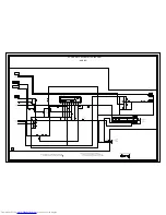
Page 25: ... 220K 1 4W R422 330K 1 4W R407 1 1 2W TP802 TP803 TP801 C418 1000 25V YK C417 22 50V YK D402 MTZJ30B D401 MTZJ30B W859 W867 L801 100uH L802 150uH 0607 L803 150uH 0607 L804 150uH 0607 L401 4 7mH 0909 D403 11E1 EIC D405 AU02A EIC D410 AU02A EIC D801 1SS133 D802 1SS133 D803 1SS133 D404 11E1 EIC D406 11E1 EIC D407 11E1 EIC D408 1SS133 C406 0 0015 500V B C442_1 0 0086 1 5KV MPP C629 0 001 B C422 0 47 1...

Page 26: ...20 6 3V YK C503 4 7 100V MHE C515 1000 25V MHE C505 150 450V LU C523 220 10V YK D511 MTZJ15B D528 MTZJ5 6B W816 W828 W847 W814 W826 W809 D507 1SS133 D505 11E1 EIC D520 30DF6 FC D515 SB10 03A3 D512 SB10 03A3 D519 1SS133 D514 1SS133 D521 1SS133 D508 1N4937 D506 1SS133 D513 SB290S D523 11E1 EIC D524 11E1 EIC D516 SB290S D501 RM11C EIC D504 RM11C EIC D502 RM11C EIC D503 RM11C EIC D526 30DF6 FC D527 11...

Page 27: ...W830 W846 W813 W841 W850 W825 D1002 1SS133 D1001 1SS133 D1003 1SS133 C1009 0 0039 B C1020 0 001 B C759 0 001 B C1016 1 F C1019 220 6 3V YK C1003 0 1 50V KA C736 1 50V KA C1011 100 16V YK C1010 2 2 50V KA C1002 100 6 3V YK C1018 100 6 3V YK C1012 470 35V MHE C757 100 10V YK C1013 1000 16V YK OF PRINTING AND SUBJECT TO CHANGE WITHOUT NOTICE NOTE THIS SCHEMATIC DIAGRAM IS THE LATEST AT THE TIME WAS R...

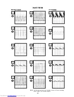
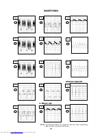
Page 28: ...g waveforms were measured at the point of the corresponding balloon number in the schematic diagram NOTE 0 5µs 1 00V 10ms 1 00V 20µs 1 00V 20µs 1 00V 50µs 100mV 0 2ms 1 00V 0 2ms 1 00V 50µs 0 50V 50µs 100mV 50µs 100mV 20µs 0 50V 20µs 1 00V 20µs 1 00V 20µs 1 00V 12 2ms 200mV H 1 ...

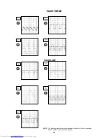
Page 29: ...easured at the point of the corresponding balloon number in the schematic diagram NOTE 20µs 1 00V 20µs 100mV 20µs 1 00V 20µs 1 00V 20µs 1 00V 20µs 1 00V 20µs 1 00V 20µs 200mV 10ms 1 00V 20µs 1 00V 16 20µs 100mV DEFLECTION CRT 33 34 10ms 1 00V 10ms 10 0V 31 2ms 200mV 30 2ms 200mV H 2 ...

Page 30: ...eforms were measured at the point of the corresponding balloon number in the schematic diagram NOTE SOUND AMP 43 2ms 0 50V 40 20µs 50V 41 20µs 50V 45 0 2ms 5 0V 37 20µs 5 0V 38 39 20µs 50V 2µs 200V 35 36 10ms 10 0V 20µs 10 0V H 3 ...

Page 31: ... 202 113 202 202 202 110 203 202 114 118 117 116 205 204 204 204 205 115 203 112 109 PCB010 MAIN PCB ASS Y 103 104 107 106 203 105 101 203 102 MECHANICAL EXPLODED VIEW I 1 111 201 201 201 201 PCB110 CRT PCB ASS Y ...

Page 32: ...C 118 752WSA0216 SHIELD CASE 201 8121J50B54 SCREW TAPPING B0 GW20 5x28 202 8117540A64 SCREW TAPPING B0 TRUSS 4x16 203 8110630A04 SCREW TAP TITE P BRAZIER 3x10 204 8109I30A04 SCREW TAP TITE B WH7 3x10 205 8107630804 SCREW TAP TITE S BRAZIER 3x8 723000C009 SHEET BAR CODE 791WHA0085 LAMIFILM BAG 792UHA0171 PACKAGE TOP 792UHA0172 PACKAGE BOTTOM 793UCDB029 GIFT BOX A3L908G975 INSTRUCTION BOOK KIT JB5XD...

Page 33: ...1 8K OHM 1 10W R519 R801R7101J RC 100 OHM 1 10W R142 R801R7182J RC 1 8K OHM 1 10W R521 R3X28BR56J R METAL OXIDE 0 56 OHM 3W R143 R801R7152J RC 1 5K OHM 1 10W R522 R002T44R7J RC 4 7 OHM 1 4W R144 R002T4102J RC 1K OHM 1 4W R523 R801R7102J RC 1K OHM 1 10W R145 R002T4102J RC 1K OHM 1 4W R524 R002T4473J RC 47K OHM 1 4W R146 R002T4102J RC 1K OHM 1 4W R527 R3X181R12J R METAL OXIDE 0 12 OHM 1W R147 R002T4...

Page 34: ... 1 4W C221 CS0RB0315K CC 0 1 UF 25V B R805 R801R7271J RC 270 OHM 1 10W C301 CS0RB0413K CC 0 001 UF 50V B R806 R801R7182J RC 1 8K OHM 1 10W C302 CS0RCH4E2J CC 150 PF 50V CH R807 R3X18A123J R METAL OXIDE 12K OHM 2W C303 CS0RB0413K CC 0 001 UF 50V B R808 R801R7221J RC 220 OHM 1 10W C304 CS0RB0413K CC 0 001 UF 50V B R809 R002T4272J RC 2 7K OHM 1 4W C305 CS0RB0315K CC 0 1 UF 25V B R810 R002T4560J RC 56...

Page 35: ...F6 FC C630 CS0RCH4S1J CC 56 PF 50V CH D521 D1VT001330 DIODE SILICON 1SS133T 77 C633 CS0RB0414K CC 0 01 UF 50V B D523 D2WT011E10 DIODE SILICON 11E1 EIC C634 E00NU2220M CE 22 UF 16 V D524 D2WT011E10 DIODE SILICON 11E1 EIC C637 CS0RCH4S1J CC 56 PF 50V CH D525 D2WT011E10 DIODE SILICON 11E1 EIC C638 CS0RB0414K CC 0 01 UF 50V B D526 D28F30DF60 DIODE RECTIFIER 30DF6 FC C640 CS0RB0414K CC 0 01 UF 50V B D5...

Page 36: ... TCATC3199Y TRANSISTOR SILICON KTC3199_Y AT CP502 069S420110 CONNECTOR PCB SIDE A1561WV2 2P Q802 TCA0042170 TRANSISTOR SILICON KTC4217 O Y CP801 069S320010 CONNECTOR PCB SIDE A2361WV2 2P Q803 TCATC3199Y TRANSISTOR SILICON KTC3199_Y AT CP1002 069S120419 CONNECTOR PCB SIDE A2502WV2 2P Q804 TCA0042170 TRANSISTOR SILICON KTC4217 O Y CP802A 067U005049 WIRE HOLDER B2013H02 5P Q805 TCATC3199Y TRANSISTOR ...

Page 37: ...TOSHIBA Information Systems UK Ltd Consumer Products Division European Service Centre Admiralty Way Camberley Surrey GU15 3DT ...

Reviews: