background image

LCD TV

SERVICE MANUAL

FILE NO.  050-200224

15

D

L72

DOCUMENT CREATED IN JAPAN, Oct., 2002

Summary of Contents for 15DL72

Page 1: ...LCD TV SERVICE MANUAL FILE NO 050 200224 15DL72 DOCUMENT CREATED IN JAPAN Oct 2002 ...

Page 2: ...nd repeat AC voltage measurements for each exposed metallic part Voltage measured must not exceed 5 25V rms This corresponds to 3 5 mA AC Any value exceeding this limit constitutes a potential shock hazard and must be corrected immediately 0 15 mF 1500 W 10W Good earth ground such as a water pipe conduit etc Place this probe on each exposed metallic part AC VOLTMETER PRODUCT SAFETY NOTICE Many ele...

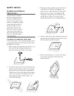
Page 3: ...eful to align the four holes at the right side and left side of the LCD module with the corresponding holes in the LCD cover before securing the module with four screws Do not force the module into place because stress can affect its performance Also the panel s polarized surface is easily scarred so be careful when handling it 3 If the panel s surface gets dirty wipe it with cotton or a soft clot...

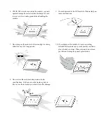
Page 4: ... long periods 8 Do not store the module at temperatures below specifications Cold can cause the liquid crystals to freeze lose their elasticity or otherwise suffer damage 9 Do not disassemble the LCD module Disassembly can cause malfunctions 10 If you transport the module do not use packing material that contains epoxy resin amine or silicon glue alcohol or oxime These materials can release gas th...

Page 5: ...PC Board 1 3 1 5 Handle 1 3 1 6 LCD Rear Cover 1 3 1 7 Wall Hanging Plate 1 4 1 8 Bottom Cover 1 4 1 9 Side Cover 1 4 1 10 Rear Terminal Panel Main PC Board 1 4 1 11 Front Net Speaker 1 5 1 12 Switch PC Board 1 5 1 13 Hinge Top Cover 1 5 3 3 Input Jack Circuit Diagram 2 11 3 4 VPC3230 Circuit Diagram 2 13 3 5 TTX Caption Circuit Diagram 2 15 3 6 MXIC Circuit Diagram 2 17 3 7 Frame Buffer Circuit D...

Page 6: ...This page is not printed ...

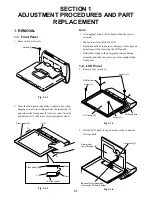
Page 7: ...Take care not to scratch the LCD Caution should be taken to avoid injury from edges on metal areas when removing the LCD panel Return the wiring to their original positions during assembly and take care not to get wires caught in the front panel 1 2 LCD Panel 1 Remove four screws 1 Fig 1 1 3 2 Lift the LCD panel 2 up and remove the connector 3 from back Screws 1 A A LCD rear panel Front panel 2 LC...

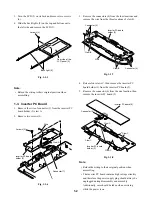
Page 8: ...r PC board holder 2 from the inverter PC board 5 5 Remove the connector 6 from the one location then remove the inverter PC board 5 Fig 1 1 8 Note Return the wiring to their original position when assembling The inverter PC board contains high voltage circuitry and therefore the power supply plug should always be unplugged during disassembly and assembly Additionally care should be taken when serv...

Page 9: ...er 1 Remove the front panel the LCD panel and the inverter PC board Refer to item 1 1 1 2 and 1 3 2 Remove two screws 1 then remove the support 2 3 Remove two screws 3 and remove the LCD rear cover 4 in a vertical position Note If not removed when in a vertical position the hinges may become deformed Fig 1 1 12 Screws 1 Connector 2 Sensor PC board 3 GND lead wire Sensor PC board 3 GND lead wire Pl...

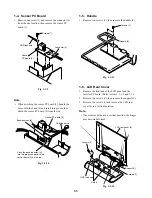
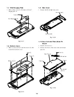
Page 10: ...r 3 Fig 1 1 14 1 9 Side Cover 1 Remove the left and right side covers Fig 1 1 15 1 10 Rear Terminal Panel Main PC Board 1 Remove two screws 1 2 Remove two claws A then remove the rear terminal panel 2 Fig 1 1 16 Screws 1 Wall Hanging Plate 2 Bottom cover 3 Screws 1 Screws 2 Side cover left Side cover right Screw 1 Screw 1 Rear terminal panel 2 GND lead wire Claw A Claw A Main PC board ...

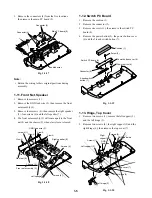
Page 11: ... one screw 3 then remove the switch PC board 4 4 Remove the power button 5 the power button cover 6 and the 5 knob switch button 7 Fig 1 1 19 1 13 Hinge Top Cover 1 Remove two screws 1 remove the left support 2 and the left hinge 3 2 Remove two screws 4 the right support 5 and the right hinge 6 then remove the top cover 7 Fig 1 1 20 Connector 4 Connector 4 Main PC board 5 Bundled wires Screws 1 GN...

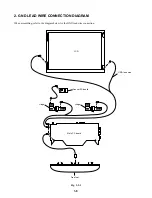
Page 12: ...1 6 2 GND LEAD WIRE CONNECTION DIAGRAM When assembling refer to the diagram below for the GND lead wire connection Fig 1 2 1 GND lead wire LCD Front net Sensor PC board Hinge Hinge Main PC board ...

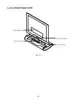
Page 13: ...1 7 3 LOCATION OF MAIN PARTS Fig 1 3 1 U002 Switch PC board U004 Inverter PC board U001 Main PC board U003 Sensor PC board ...

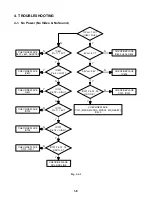
Page 14: ... CHECK REPLACE X201 IC201 3 3Vcc 3 3V IC201 Pin 34 35 OSC O K IC801 Pin 1 12V IC801 Pin 4 LOW IC701 Pin 19 HIGH IC701 Pin 11 5V IC701 Pin 18 HIGH IC701 Pin 13 14 OSC O K CHECK REPLACE SCL SDA LINE CHECK REPLACE F801 L801 ADAPTER CHECK REPLACE IC801 CHECK REPLACE Q801 CHECK REPLACE IC702 CHECK REPLACE IC704 CHECK REPLACE X701 IC701 CHECK REPLACE IC201 MXCS MXSDA MXSCL MX_RESET IC400 ...

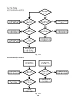
Page 15: ...301 OUTPUT O K IC301 Pin 3 3V CHECK REPALCE LCD PANEL INTERFACE CABLE IC101 Pin 62 63 OSC O K 4 2 No Video 4 2 1 No Video Sound O K Fig 1 4 2 4 2 2 No Video Sound O K Fig 1 4 3 Y N N Y N Y RF MODE O K A V MODE NG RF MODE N G A V MODE O K CHECK REPLACE IC101 D104 L105 CHECK REPLACE IC501 IC601 CHECK REPLACE TU1 Q502 CHECK REPLACE IC502 Q501 IC601 IC501 Pin 7 SIGNAL O K IC502 Pin 3 SIGNAL O K CHECK ...

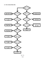
Page 16: ...K REPLACE SPEAKER WIRE CHECK REPLACE IC681 R681 CHECK REPLACE IC681 Q681 Q682 Q683 IC601 Pin 39 8V IC601 Pin 21 A_RESET HIGH IC601 Pin 71 72 OSC O K IC601 Pin 47 48 INPUT O K IC601 Pin 33 34 OUTPUT O K IC601 INPUT O K CHECK AUDIO INPUT JACK CHECK REPLACE IC601 L601 L602 CHECK REPLACE IC802 CHECK REPLACE IC601 X601 CHECK REPLACE IC701 IC601 CHECK REPLACE IC601 CHECK REPLACE IC651 CHECK REPLACE IC60...

Page 17: ...amic capacitor described 1 3 Capacitance Indication Table 2 1 3 Fig 2 1 3 1 4 Waveform and Voltage Measurement The various wave forms of the color circuit and voltage measurement values are for when the service color bar signal is received with ample reception and a proper image is received Other various wave forms of circuits and voltage measurement values are for when general broadcasts are norm...

Page 18: ...2 2 12VCC FET_SW VIN 8VCC INVERTOR SOUND AMP DC12V IC801 IC702 POWER IC702 F801 IC803 3 3VCC 5VM 5V REG 8V REG 5VCC 5V REG IC804 3 3V REG 2 BLOCK DIAGRAMS 2 1 Power Block Diagram Fig 2 2 1 ...

Page 19: ...2 3 REMOTE PCB STANDBY LED IC701 MAIN_SW KEY_IN1 CN801 MAIN_SW POWER LED STANDBY LED POWER LED CN701 KEY_IN1 INVERTOR PCB 21 1 MICROPROCESSOR 2 2 Inverter Block Diagram Fig 2 2 2 ...

Page 20: ...LECT PANEL POWER CONTROL Key Input N C N C In Out Input Input Input Input Input Output Input Input Output Output Output Output Output Output Output Output Input Output Output Output Output Output Output Logic Active Low Active Low Active Low Active High Active High Active Low Active Low Active High Active Low Active Low Active Low Active High ADC ACTIVE HIGH ACTIVE HIGH Active High Active Low Acti...

Page 21: ... 10 RCA A1 Audio Video2 R RCA V1 RCA V1 NJM2233B AUDIO PROCESSOR IIC BUS RCA A1 B 0 7 TXC TXC IMAGE SCALER RCA V2 CAPTION RGB F B NJM2700 TX3 TX3 RCA CVBS VIDEO SW AUDIO AMP TV CVBS RCA A2 IIC BUS HS RCA DVD CVBS TX0 TX0 VS TUNER DS90C385 SP MAIN L TX1 TX1 SVHS MX88L284 H MAIN R SVHS Y SDRAM FRAME MEMORY CAPTION RCA V2 Y 0 7 SVHS C V Z86129 LVDS C 0 7 L RCA A2 Fig 2 2 3 2 6 2 5 ...

Page 22: ... 2 3 4 5 6 7 8 D802 MBRS340 2 1 D801 EC10DS1 2 1 IC803 LM2596S 5 0 1 2 3 4 5 IN OUT GND F B ON OFF C801 220uF 16V DIP C807 220uF 16V DIP Q801 BC848 1 3 2 IC801 FDS4435 C 1 2 3 4 5 6 7 8 S S S GD D D D L801 ZJR5101 102 1 3 2 A B C JA801 HEC3800 01 0 10 1 2 3 C802 100nF L802 N2012ZA400T06 C803 100nF L803 N2012ZA400T06 F801 A TSC 5A C805 100nF C816 220uF 16V DIP C811 220uF 16V DIP C815 220uF 16V DIP ...

Page 23: ...20 4 7K RC4 390 C716 47pF 47pF R725 560 C712 33pF D701 UDZS4 7B 2 1 SC4 TACT SW CN703 2 1 3 4 5 R722 1K R705 33K R709 100 R727 560 CN702 BSB PH K S 1 2 3 4 5 6 7 8 R718 100 R707 22K R708 2 7K R728 560 Q702 BC848 1 3 2 R719 100 R704 2 7K Q701 BC848 1 3 2 RC2 1 3K R731 CB2012GA221 C706 100nF C704 100nF IC701 KS88C6348 33 34 35 36 37 38 39 40 41 42 19 1 20 17 2 3 21 18 22 23 24 25 26 27 28 29 30 31 3...

Page 24: ... 1T2012 330JT R525 1K JA502 YKC21 5856 N 1 4 2 3 5 6 R517 100 R514 75 L512 EF 1T2012 330JT R528 100 R510 75 IC501 NJM2233BV 1 3 2 4 5 6 7 8 VIN1 VIN2 SW1 NC NC V V OUT GND L506 EF 1T2012 330JT D502 UDZS4 7B 2 1 R512 75 R502 470K C504 47uF 16V R505 82 C501 100nF C502 10uF 16V C505 47uF 16V R506 82 L503 FI A2012 331KJ T 1 2 3 4 5 6 7 8 9 10 11 12 13 14 15 16 17 18 19 NC0 9V AGC VT VCC1 SCL SDA AS NC...

Page 25: ...TLC VREF AVO FB1IN FSY HC AISGND MSY HS VS FPDAT VSTBY CLK5 NC XTAL1 XTAL2 ASGF GNDPA VSUPPA LLC2 LLC1 VSUPLLC GNDLLC Y7 Y6 Y5 Y4 GNDY VSUPY Y3 Y2 Y1 Y0 B1 CB1IN G1 Y1IN R1 CR1IN B2 CB2IN G2 Y2IN R2 CR2IN ASGF NC VSUPCAP VSUPD GNDD GNDCAP SCL SDA RESQ TEST VGAV YCOEQ FFIE FFWE FFRSTW FFRE FFOE CLK20 D106 UDZS 4 7B 2 1 D101 UDZS4 7B 2 1 L104 FI B2012 222KJ T L113 FI B2012 222KJ T D105 UDZS4 7 B 2 1...

Page 26: ... 150 RX15 1K LZ 1 FI A2012 331KJT RZ1 1K CZ4 100nF CZ6 6 8nF CX7 47p F RX 5 1K CZ3 560pF RZ6 10K RX10 240 RZ4 0 RX9 240 RX14 1K RZ3 0 RZ2 0 CZ2 10uF 16V 2 150 CZ1 100nF RZ7 6 8 K RZ5 0 RX2 100 RX8 240 ICZ1 Z86129_DIP 17 18 1 2 10 11 12 13 14 15 16 3 4 5 6 7 8 9 F B R OUT Vss G OUT RREF Vss A Vdd Vin INTRO SDA SCL SDO B OUT SEN HIN SMS CVBS CSYNC LPF RX12 3 5 TTX Caption Circuit Diagram 2 16 2 15 F...

Page 27: ...10uF 16V C274 56pF C242 56pF C214 100nF C231 56pF R203 CBA3216GA301N4 1 5 8 4 3 7 6 2 C218 100nF IC201 MX88L284AEC 108 109 110 111 112 113 114 115 116 117 118 119 120 121 122 123 124 125 126 127 128 129 130 131 132 133 134 135 136 137 138 139 140 141 142 143 144 145 146 147 148 149 150 151 152 153 154 155 156 53 54 55 56 57 58 59 60 61 62 63 64 66 67 68 70 71 72 73 74 75 76 77 78 79 80 81 82 83 84...

Page 28: ...7 V161610DTC 8 26 27 28 29 30 31 32 33 34 35 36 37 38 39 40 41 42 43 44 45 46 47 48 49 50 1 2 3 4 5 6 7 8 9 10 11 12 13 14 15 16 17 18 19 20 21 22 23 24 25 VSS A4 A5 A6 A7 A8 A9 N C CKE CLK UDQM N C VDDQ DQ8 DQ9 VSSQ DQ10 DQ11 VDDQ DQ12 DQ13 VSSQ DQ14 DQ15 VSS VDD DQ0 DQ1 VSSQ DQ2 DQ3 VDDQ DQ4 DQ5 VSSQ DQ6 DQ7 VDDQ LDQM WE CAS RAS CS A11 A10 A0 A1 A2 A3 VDD C255 100nF C256 1 0 0nF C2 62 1 0 0nF C2...

Page 29: ...L302 4 7 u H 2A4 C310 15 pF IC301 DS90C385MTD 51 52 54 55 56 2 3 4 6 7 8 10 11 12 14 15 16 18 19 20 22 23 24 25 27 28 30 31 17 37 38 41 42 45 46 47 48 40 39 50 1 9 26 44 34 5 13 21 29 53 36 43 49 33 35 32 D0 D1 D2 D3 D4 D5 D6 D7 D8 D9 D10 D11 D12 D13 D14 D15 D16 D17 D18 D19 D20 D21 D22 D23 D24 D25 D26 CLKIN CLKSEL Y3P Y3M Y2P Y2M Y1P Y1M Y0P Y0M CLKOUTM CLKOUTP D27 VCC VCC VCC LVDSVCC PLLVCC GND G...

Page 30: ...SUP NC AVSUP NC ANA_IN1 AHVSS ANA_IN AHVSS ANA_IN2 AGNDC TESTEN NC XTAL_IN SC4_IN_L XTAL_OUT SC4_IN_R TP ASG4 AUD_CL_OUT SC3_IN_L NC SC3_IN_R NC ASG2 D_CTR_OUT1 SC2_IN_L D_CTR_OUT0 SC2_IN_R ADR_SEL ASG1 STANDBYQ SC1_IN_L SC1_IN_R VREFTOP NC MONO_IN AVSS AVSS NC NC DACA_L VREF2 DACM_R DACM_L NC DACM_SUB NC ASG3 SC2_OUT_R SC2_OUT_L VREF1 SC1_OUT_R SC1_OUT_L CAPL_A AHVSUP CAPL_M NC I2C_CL I2C_DA I2S_...

Page 31: ...6 7 8 9 10 11 12 13 14 15 16 17 18 19 20 21 22 23 24 47 48 45 46 INR INL C3 C4 NC MODE1 TP2 BASSOUT OUTR OUTL FFR4 FFR3 FFR2 FFR1 FFL4 NC NC FFL3 FFL2 FFL1 NC FIL3 FIL4 FIL5 FIL6 FIL7 PCOUT PCIN C1 C2 SFIL2 NC NC SFIL2 SFIL3 SVOL2 SVOL1 GND VCC VREFIN VREF MODE3 MODE2 NC FIL2 NC FILOUT FIL1 C6 62 39nF C6 61 10uF 16V C6 65 3 9nF C6 68 10nF L651 FI A2 012 331KJT R662 82K R658 130K R6 57 9 1 K R651 1...

Page 32: ...V DIP C6 89 1000 u F 16V R6 89 8 2 K R6 87 C684 1000u F 16V C6 92 1uF 50V L681 N2012ZA400T06 R6 88 1K R695 22K R684 10 C687 100nF IC681 TDA1517 3 8 5 9 6 2 1 4 7 Vref Mute GND Rin OUT_R S_GND Lin OUT_L Vcc 12 R685 24K R6 83 8 2 K C6 81 2200u F 16V R6 82 1K C691 100nF C688 1uF 50V C690 330pF C683 1uF 50V R690 10 Q681 BC848 1 3 2 C685 330pF JA681 YKB21 5101A 5 4 2 3 7 1 8 CN681 B4B EH 1 2 3 4 HW220 ...

Page 33: ... 0V 24 1 7V 3 0V 7 0V 4 0V 25 5V 4 0V 8 12V 5 5V 26 5V 6 5V 27 5V 7 5V 28 5V PIN VOLTAGE PIN VOLTAGE 8 5V 29 0V 1 0V 5 4 2V 9 0V 30 0V 2 0V 6 4 4V 10 5V 31 5V 3 0V 7 0V 11 5V 32 0V 4 0V 8 5V 12 0V 33 0V 13 2 8V 34 5V 14 2 7V 35 4 8V 15 0V 36 0V 16 0V 37 5V 17 0V 38 5V 18 5V 39 3 9V 19 5V 40 4 2V 20 5V 41 4 4V 21 5V 42 0V IC702 MC78L05 PIN VOLTAGE Microprocessor Circuit Page 2 9 IC703 24C16 PIN VOL...

Page 34: ...55 3 0V 2 NC 11 NC 16 0V 56 1 4V 3 NC 12 NC 17 0V 57 3 2V 4 NC 13 NC 18 0V 58 3 3V 5 4 84V 14 NC 19 2 8V 59 5V 6 4 4V 15 2V 20 2 8V 60 3 5V 7 4 2V 16 2 9V 21 0V 61 0V 8 0V 17 4 84V 22 0V 62 2 8V 9 NC 18 NC 23 0V 63 2 6V 24 2 4V 64 0V 25 0V 65 0V 26 3 3V 66 2 5V 27 2 2V 67 5V 28 2 4V 68 0V 29 3 3V 69 5V 30 0V 70 1 7V 31 2V 71 1 5V 32 2V 72 1 5V 33 2V 73 1 4V 34 2V 74 1 4V 35 0V 75 1 4V 36 3 3V 76 5...

Page 35: ... 17 0V 43 0V 18 0V 44 3 3V 19 0V 45 0V 20 0V 46 0V 21 0V 47 0V 22 0V 48 0V 23 1 1V 49 4 2V 24 0V 50 4 4V 25 0 7V 51 0V 26 1 2V 52 0V PIN VOLTAGE PIN VOLTAGE 1 0V 5 5V 2 0V 6 5V 3 0V 7 0V 4 0V 8 5V PIN VOLTAGE PIN VOLTAGE 1 3 6V 9 0V 2 0V 10 0V 3 3 6V 11 3V 4 3 6V 12 0V 5 3 6V 13 3V 6 3 6V 14 12V 7 3 6V 15 0V 8 0V 16 3V ICX1 SAA5264 PIN VOLTAGE ICX2 24C02 PIN VOLTAGE ICS1 TEA5114 PIN VOLTAGE TTX CA...

Page 36: ...V 127 2 5V 179 0V 24 2 3V 76 1 7V 128 2 5V 180 0V 25 0V 77 1 7V 129 2 5V 181 0V 26 0V 78 1 7V 130 2 5V 182 0V 27 0V 79 1 7V 131 2 5V 183 4 8V 28 0V 80 1 7V 132 2 5V 184 4 9V 29 0V 81 1 7V 133 2 5V 185 4 9V 30 0V 82 1 7V 134 0V 186 0V 31 0V 83 1 7V 135 2V 187 3 2V 32 0V 84 1 7V 136 0V 188 3 2V 33 0V 85 1 7V 137 1 7V 189 2 3V 34 2 1V 86 1 7V 138 3 3V 190 0V 35 2 8V 87 1 7V 139 1 5V 191 2 3V 36 3 3V ...

Page 37: ... 11 2 4V 36 2 2V 11 2 4V 36 2 2V 12 2 4V 37 0V 12 2 4V 37 0V 13 3 3V 38 3 3V 13 3 3V 38 3 3V 14 2 3V 39 3 2V 14 2 3V 39 3 2V 15 3 5V 40 3 2V 15 3 5V 40 3 2V 16 3 6V 41 0V 16 3 6V 41 0V 17 3 6V 42 3 1V 17 3 6V 42 3 1V 18 0V 43 3 0V 18 0V 43 3 0V 19 3 3V 44 3 3V 19 3 3V 44 3 3V 20 2 3V 45 3 0V 20 2 3V 45 3 0V 21 3 3V 46 3 0V 21 3 3V 46 3 0V 22 3 4V 47 0V 22 3 4V 47 0V 23 3 1V 48 2 7V 23 3 1V 48 2 7V...

Page 38: ...3 7V 18 1 7V 46 1 4V 18 0V 58 3 7V 19 1 7V 47 1 3V 19 0V 59 0V 20 1 7V 48 1 4V 20 0V 60 3 7V 21 0V 49 0V 21 3 8V 61 0V 22 1 7V 50 1 7V 22 0V 62 0V 23 1 7V 51 1 7V 23 0V 63 0V 24 1 7V 52 1 7V 24 0V 64 0V 25 0V 53 0V 25 0V 65 4 9V 26 3 3V 54 1 7V 26 0V 66 4 9V 27 2 2V 55 1 7V 27 1 5V 67 1 6V 28 0 3V 56 1 7V 28 1 5V 68 0V 29 0V 69 0V 30 2 1V 70 0V PIN VOLTAGE PIN VOLTAGE 31 0V 71 2 9V 1 3 26V 5 3 25V...

Page 39: ... 12V 0V 8V 12 0V 36 0V IC804 0V 3 3V 5V 13 0V 37 0V IC704 5V 0V 5V 14 6 0V 38 0 9V ICM1 5V 4 46V 0V 15 6 0V 39 0 9V DC1 0V 0V 0V 16 6 0V 40 0 9V 17 6 0V 41 0 9V 18 0V 42 0 9V LOC Pin1 Pin2 19 12V 43 0 9V NO 20 6 0V 44 0 9V DC2 2 8V 5 5V 21 6 0V 45 0 9V DC3 0V 2 8V 22 4 6V 46 0 9V DC4 5 5V 2 8V 23 4 6V 47 0 9V DC5 2 8V 0V 24 0V 48 0V D681 12V 4V IC651 NJM2700 PIN VOLTAGE WOW Control Circuit Page2 2...

Page 40: ... Circuit Page 2 7 IC701 PIN14 Microprocessor Circuit Page 2 9 IC701 PIN24 Microprocessor Circuit Page 2 9 IC701 PIN23 Microprocessor Circuit Page 2 9 IC701 PIN22 Microprocessor Circuit Page 2 9 IC701 PIN41 Microprocessor Circuit Page 2 9 ...

Page 41: ...2 37 IC701 PIN40 Microprocessor Circuit Page 2 9 TU1 PIN16 Input Jack Circuit Page 2 11 TU1 PIN15 Input Jack Circuit Page 2 11 ...

Page 42: ...2 38 IC101 PIN62 VPC3230 Circuit Page 2 13 IC101 PIN73 VPC3230 Circuit Page 2 13 IC101 PIN28 VPC3230 Circuit Page 2 13 IC101 PIN56 VPC3230 Circuit Page 2 13 IC101 PIN57 VPC3230 Circuit Page 2 13 ...

Page 43: ...2 39 IC201 PIN35 MXIC Circuit Page 2 17 IC201 PIN101 MXIC Circuit Page 2 17 IC201 PIN70 MXIC Circuit Page 2 17 IC201 PIN99 MXIC Circuit Page 2 17 IC201 PIN100 MXIC Circuit Page 2 17 ...

Page 44: ...2 40 IC601 PIN33 34 Sound Circuit Page 2 23 IC601 PIN27 28 Sound Circuit Page 2 23 IC651 PIN29 30 WOW Control Circuit Page 2 25 IC681 PIN6 4 Sound AMP Circuit Page 2 27 ...

Page 45: ...10 1 3 4 A B C D E G 2 5 6 7 8 9 F 4 PC BOARDS 4 1 Main PC Board Fig 2 4 1 U001 Main PC board Top side 2 42 2 41 ...

Page 46: ...10 1 3 4 A B C D E G 2 5 6 7 8 9 F Fig 2 4 2 U001 Main PC board Bottom side 2 44 2 43 ...

Page 47: ...G 2 5 F 2 45 4 2 Switch PC Board 4 3 Sensor PC Board Fig 2 4 3 U002 Switch PC Board Top side Fig 2 4 4 U002 Switch PC Board Bottom side Fig 2 4 5 U003 Sensor PC Board Top side Fig 2 4 6 U003 Sensor PC Board Bottom side ...

Page 48: ...2 46 This page is not printed ...

Page 49: ...assist in processing be sure to include the model number and description ABBREVIATIONS 1 Integrated Circuit IC 2 Capacitor Cap Capacitance Tolerance for Nominal Capacitance more than 10pF P 100 0 Symbol Tolerance B 0 1 C 0 25 D 0 5 F 1 G 2 J 5 K 10 M 20 N 30 V 20 10 W 100 10 U 75 10 Q 30 10 T 50 10 Symbol Tolerance X 40 20 Y 150 10 Z 80 20 Ex 10µF J 10µF 5 Symbol Tolerance pF B 0 1 C 0 25 D 0 5 F ...

Page 50: ...3 2 4 EXPLODED VIEWS 4 1 Packing Assembly Fig 3 4 1 M001 A702 A702 A702 A702 Y101A Y101B A702 Y106 P802 A703 A701 ...

Page 51: ...02 B205 A205 A503 A301 U002 A501 A502 A203 A206 W661 A302 A302 U001 TU1 A204 U003 A401 A201 B212 B212 B212 A351 A351 B217 B215 B215 B216 B216 B212 A350 B212 B212 B212 B213 B214 B214 B211 A303 B218 4 2 Chassis Assembly Fig 3 4 2 ...

Page 52: ...S4 7B MM3Z4V7T1 D108 72790269 ZENER DIODE UDZS4 7B MM3Z4V7T1 D201 72790276 LED RED 3P SLR 342VC T32 D501 72790269 ZENER DIODE UDZS4 7B MM3Z4V7T1 D502 72790269 ZENER DIODE UDZS4 7B MM3Z4V7T1 D601 72790267 ZENER DIODE UDZS5 1B MM3Z5V1T1 D602 72790267 ZENER DIODE UDZS5 1B MM3Z5V1T1 D603 72790267 ZENER DIODE UDZS5 1B MM3Z5V1T1 D604 72790267 ZENER DIODE UDZS5 1B MM3Z5V1T1 D605 72790267 ZENER DIODE UDZS...

Page 53: ...2790262 INDUCTOR SMD FI B2012 222KJT L113 72790262 INDUCTOR SMD FI B2012 222KJT L201 72790261 INDUCTOR SMD FI A2012 331KJT L202 72790261 INDUCTOR SMD FI A2012 331KJT L203 72790261 INDUCTOR SMD FI A2012 331KJT L301 72790261 INDUCTOR SMD FI A2012 331KJT L302 72790264 POWER INDUCTOR SMD 47UH 2A4 L303 72790261 INDUCTOR SMD FI A2012 331KJT L304 72790261 INDUCTOR SMD FI A2012 331KJT L501 72790258 EMI FI...

Page 54: ...B HB 4M3216 301JT R210 72790274 NET FERRITE B HB 4M3216 301JT R211 72790272 FERRITE BEAD HB 1M2012 221JT R212 72790272 FERRITE BEAD HB 1M2012 221JT R219 72790275 NETWORK BEAD R220 72790275 NETWORK BEAD R221 72790275 NETWORK BEAD R222 72790275 NETWORK BEAD R223 72790275 NETWORK BEAD R224 72790275 NETWORK BEAD R225 72790275 NETWORK BEAD R226 72790272 FERRITE BEAD HB 1M2012 221JT R228 72790272 FERRIT...

Page 55: ...ts No Description X601 72790257 X TAL 18 432MHZ 15PF SMD X701 72790254 X TAL 12MHZ 56PF SMD XX1 72790254 X TAL 12MHZ 56PF SMD Y101A 72790348 OWNER S MANUAL A Y101B 72790349 OWNER S MANUAL B Y106 72790333 REMOCON USA CT 842 3 7 ...

Page 56: ...3 8 This page is not printed ...

Page 57: ...TOSHIBA CORPORATION 1 1 SHIBAURA 1 CHOME MINATO KU TOKYO 105 8001 JAPAN ...

Reviews: