


THCV235_THCV236_Rev.3.40_E
Copyright
©
2016 THine Electronics, Inc.
THine Electronics, Inc.
39/68
Security E
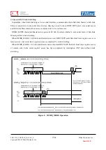
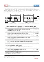
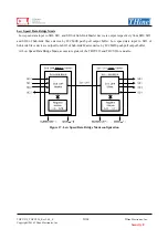
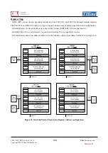
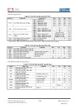
Low Speed Data Bridge Mode
Low speed data input to SD2, SD1 and SD0 of Sub-Link Master device is output respectively from SD2, SD1
and SD0 of Sub-Link Slave device by LVCMOS push pull output buffer. Low speed data input to SD3 of
Sub-Link Slave device is output from SD3 of Sub-Link Master device by LVCMOS push pull output buffer.
At Low Speed Data Bridge Mode, access to register of the THCV235 and THCV236 is unable.
Figure 17.
Low Speed Data Bridge Mode configuration


