


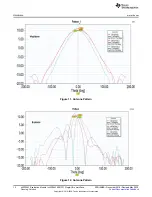


Hardware
6
SPRUIM4B – December 2018 – Revised May 2020
Copyright © 2018–2020, Texas Instruments Incorporated
xWR1843 Evaluation Module (xWR1843BOOST) Single-Chip mmWave
Sensing Solution
2.3
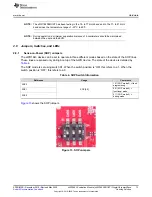
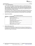
Connectors
2.3.1
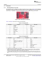
20-Pin BoosterPack Connectors
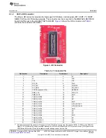
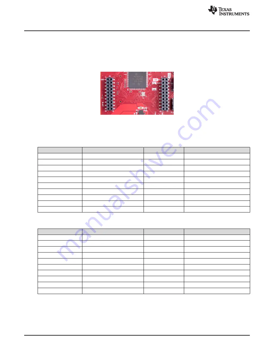
The BoosterPack has the standard LaunchPad connectors (J5 and J6, shown in
) that enable it to
be directly connected to all TI MCU LaunchPads. While connecting the BoosterPack to other LaunchPads,
ensure the pin-1 orientation is correct by matching the 3V3 and 5-V signal marking on the boards.
Figure 5. 20-Pin BoosterPack Connectors
and
provide the connector-pin information.
Table 1. J5 Connector Pin
Pin Number
Description
Pin Number
Description
1
NERROUT
2
GND
3
NERRIN
4
DSS LOGGER
5
MCUCLK OUT
6
SPI_CS
7
NC
8
GPIO01
9
MSS LOGGER
10
nRESET
11
WARMRST
12
SPI_MOSI
13
BSS LOGGER
14
SPI_MISO
15
SOP2
16
HOSTINT
17
SOP1
18
GPIO02
19
SOP0
20
NC
(1)
Voltage input to the GPADC available on the xWR1843.
(2)
Indicates the state of the onboard VIO supply for the AWR device coming from the onboard PMIC. A HIGH on the PGOOD
signal (3.3 V) indicates the supply is stable. Because the I/Os are not failsafe, the MCU must not drive any I/O signals to the
AWR device before this I/O supply is stable to avoid leakage current into the I/Os.
(3)
Controls the onboard PMIC enable. The MCU can use this to shut down the PMIC and AWR device during the periods it does
not use the AWR device and save power. The power up of the PMIC takes approximately 5 ms once the enable signal is made
high.
Table 2. J6 Connector Pin
Pin Number
Description
Pin Number
Description
1
3V3
2
5 V
3
NC
4
GND
5
RS232RX (Tx from AWR device)
6
ANA1
(1)
7
RS232RX (Rx into AWR device)
8
ANA2
(1)
9
SYNC_IN
10
ANA3
(1)
11
NC
12
ANA4
(1)
13
SPI_CLK
14
PGOOD (onboard VIO)
(2)
15
GPIO0
16
PMIC Enable
(3)
17
SCL
18
SYNC_OUT
19
SDA
20
PMIC CLK OUT