DAC and ADC GUI Configuration File Changes When Using a Xilinx Development Platform
22
SLAU580B – June 2014 – Revised September 2016
Copyright © 2014–2016, Texas Instruments Incorporated
TSW14J10 FMC-USB Interposer Card
Setup the hardware per the
ADC32RFxx EVM User’s Guide
(
) in the section titled
ADC32RFxx
Quick-Start Procedure (5-Sample Mode)
but use two synchronized external 2-GHz clock sources for the
input to J7 and J5.
Configure the ADC32RF45EVM for LMFS = 82820 mode, per steps 1–9 of the
ADC32RFxx EVM User’s
Guide
using the ADC32RFxx GUI.
After the ADC32RFx EVM has been configured, click on the
LMK04828
tab. Next, click on the
Clock
Outputs
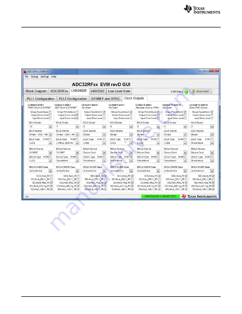
tab. The GUI appears as shown in
Figure 14. ADC32RFxx GUI LMK0828 Clock Outputs Tab
For this example, the lane rate is 8 Gbps. Using the equation in
for lane rates greater than 3.2
Gbps:
Reference clock
= Lane Rate / 20
8G / 20
= 400 MHz
Core clock
= Lane Rate / 40
8G / 40
= 200 MHz
In the ADC32RFxx GUI, the ADC REFCLK and SYSREF are provided by CLKout 2 and 3. The FPGA
Reference clock and SYSREF are provided by CLKout 0 and 1. The FPGA Core clock (for Xilinx platforms
only) is provided by CLKout 12. Notice that the default setting for CLKout 12 is
Group Powerdown
.
To generate a Reference clock = 400 MHz, set the DCLK Divider to 5 for CLKout 0. To generate a Core
clock = 200 MHz, set the DCLK Divider to 10 for CLKout 12 and unselect the
Group Powerdown
option for
this clock. The GUI will now appear as shown in


