Texas Instruments TRF4900 User Manual Download Page 22

Serial Interface and PC Port Pin Out

2-11

Evaluation Board

2.4

Serial Interface and PC Port Pin Out

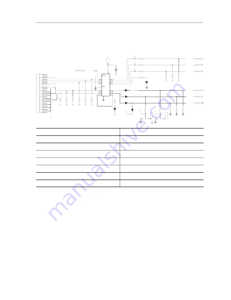
Figure 2−2 details the serial interface portion of the TRF4900 EVM.

Figure 2−2. TRF4900 EVM Serial Interface

10k

R19

10k

R20

10k

R21

17

4

16

3

15

2

14

1

13

25

12

24

11

23

10

22

9

21

8

20

7

19

6

18

5

P1

DB25M

VCC2

CLOCK

STROBE

0.1uF

C14

1

1OE

20

2

1A1

4

1A2

6

1A3

8

1A4

19

2OE

11

2A1

9

2Y1

12

1Y4

18

1Y1

16

1Y2

14

1Y3

13

2A2

15

2A3

17

2A4

7

2Y2

5

2Y3

3

2Y4

10

IC2

SN74LVT244BDW

LED2
ENABLE

LN1471SY−(TR)

10k

R23

10k

R22

10k

R24

R25

510

100

R27

100

R26

10k

R30

10k

R29

10k

R28

VCC2

VCC2

TXDATA

MODE

STDBY

LL4148

CR1

LL4148

CR2

LL4148

CR3

LL4148

CR4

2

3

1

JP2

2

3

1

JP3

MODE

STDBY

TXDATA

CLOCK

DATA

STROBE

LED1
LDET
LN1371SG−(TR)

DATA

10k

R16

10k

R17

10k

R15

100

R13

100

R12

100

R14

510

R18

LOCKDET

P1 Computer Interface Connector Pin Number

Function

2

DATA

3

CLOCK

4

STROBE

5

MODE

7

STDBY

9

TXDATA

18 thru 25

Ground

Summary of Contents for TRF4900

Page 1: ...April 2001 Mixed Signal RF Products User s Guide SWRU003B...

Page 2: ...esign TI does not warrant or represent that any license either express or implied is granted under any patent right copyright mask work right or other intellectual property right of TI covering or rel...

Page 3: ...WHATSOEVER ARISING AS A RESULT OF THE USE OF THESE BOARDS The fee associated with the evaluation modules EVM is a partial nonrecurring engineering fee NRE to partially defray the engineering costs ass...

Page 4: ...hapters Chapter 1 Overview Chapter 2 Evaluation Board Chapter 3 Software User s Guide Information About Cautions and Warnings This book may contain cautions and warnings This is an example of a cautio...

Page 5: ...iv...

Page 6: ...el Port 2 12 2 6 Jumper Connections 2 13 2 6 1 Jumper Description 2 13 2 7 Connectors and Test Points 2 14 2 7 1 Connectors 2 14 2 7 2 Test Points TP 2 14 2 7 3 Adjustments 2 15 2 7 4 LED Indicators 2...

Page 7: ...Section 3 9 3 5 Main Program Screen 3 10 3 6 Chip Layout Screen 3 11 3 7 Spectrum Analyzer 3 12 3 8 Input of Frequency Error 3 13 3 9 Main Panel Display After Clock Offset Is Applied 3 13 3 10 Chip La...

Page 8: ...1 1 Overview This chapter provides an overview of the TRF4900 evaluation module EVM Topic Page 1 1 Purpose 1 2 1 2 EVM Setup 1 2 1 3 Block Diagram 1 3 Chapter 1...

Page 9: ...evaluate the TRF4900 Step 2 Copy the TRF4900 exe file to the hard drive Step 3 Connect a DB25 female to a DB25 male cable between the TRF4900 evaluation board and the PC parallel port The DB25 female...

Page 10: ...1 2 3 4 24 22 21 20 19 17 18 23 5 6 7 8 9 10 11 12 13 14 15 16 VCO TRF4900 PLL PD_OUT2 PD_OUT1 PLL_VCC PD_SET VCO_TANK1 VCO_TANK2 PLL_GND DIG_GND CLOCK DATA STROBE MODE STDBY LOCKDET PA_OUT PA_GND PA...

Page 11: ...1 4...

Page 12: ...and its operation Topic Page 2 1 Schematics 2 2 2 2 Parts List 2 6 2 3 EVM DC Voltage Setup 2 10 2 4 Serial Interface and PC Port Pin Out 2 11 2 5 Standard PC Parallel Port 2 12 2 6 Jumper Connections...

Page 13: ...0nH LQW1608 TP1 VCC1 0 1uF C3 R2 100k 470pF C2 LOCKDET LDET STDBY TXDATA MODE CLOCK DATA STROBE 3 PD_SET 2 PLL_VCC 1 PD_OUT1 4 VCO_TANK1 5 VCO_TANK2 6 PLL_GND 7 DIG_GND 8 CLOCK 9 DATA 10 STROBE 11 MOD...

Page 14: ...25 12 24 11 23 10 22 9 21 8 20 7 19 6 18 5 P1 DB25M RED 8 0V VCC2 CLOCK STROBE 0 1uF C14 2 0 3 8V 3 0V TYP 1 1OE 20 2 1A1 4 1A2 6 1A3 8 1A4 19 2OE 11 2A1 9 2Y1 12 1Y4 18 1Y1 16 1Y2 14 1Y3 13 2A2 15 2...

Page 15: ...Top Side Silkscreen and Drawing 2 4 2 1 1 Top Side Silkscreen and Drawing...

Page 16: ...Top Side Silkscreen and Drawing 2 5 Evaluation Board 2 1 2 Bottom Side Silkscreen and Drawing...

Page 17: ...RIES Trimmer capacitor Johanson 9341 3SL Newark 95F9901 3 C4 3 3 pF 0603 Ceramic chip capacitor Venkel C0603COG500 3R3CNB Venkel C0603COG500 3R3CNB 3 C8 3 3 pF 0603 Ceramic chip capacitor Venkel C0603...

Page 18: ...on Components 142 0701 801 Newark 90F2624 2 JP2 Jumper 3 pin Breakaway headers AMP 4 103239 0 Newark 90F7725 2 JP3 Jumper 3 pin Breakaway headers AMP 4 103239 0 Newark 90F7725 1 L1 6 8 nH 0603 Surface...

Page 19: ...603 Chip resistor Venkel CR0603 16W 103JB Venkel CR0603 16W 103JB 1 R3 51 0603 Chip resistor Venkel CR0603 16W 510JB Venkel CR0603 16W 510JB 6 R4 100 0603 Chip resistor Venkel CR0603 16W 101JB Venkel...

Page 20: ...point Color coded PC test point white Components Corp TP 105 01 09 Newark 97B3253 8 DATA WHT PC test point Color coded PC test point white Components Corp TP 105 01 09 Newark 97B3253 LDET WHT PC test...

Page 21: ...nal 3 of LM317 should be 2 V to 3 V higher than Vout V 7 2 V equal to 8 V nominal With V 1 2 4 R33 LED3 VCC LN1271R TR 0 JP4 R31 C17 C18 C19 2 0 3 8 V 3 0 V TYP VCC2 3 3V C22 C21 C20 R35 VCC1 S1JB CR5...

Page 22: ...6 1A3 8 1A4 19 2OE 11 2A1 9 2Y1 12 1Y4 18 1Y1 16 1Y2 14 1Y3 13 2A2 15 2A3 17 2A4 7 2Y2 5 2Y3 3 2Y4 10 IC2 SN74LVT244BDW LED2 ENABLE LN1471SY TR 10k R23 10k R22 10k R24 R25 510 100 R27 100 R26 10k R30...

Page 23: ...ata 1 Data 2 Data 3 Data 4 Data 5 Data 6 Data 7 ACK Busy Paper Empty Select Auto Feed Error Initialize Printer Select Input PC Output PC Output PC Output PC Output PC Output PC Output PC Output PC Out...

Page 24: ...o test the tuning range of the VCO tank circuit with an external power supply The default state for jumper JP1 is JP1 1 to JP1 2 Jumper JP1 is a 0 0603 resistor JP2 Jumper JP2 can be used to pull the...

Page 25: ...used to form a T attenuator The components for this option are not installed on the EVM 2 7 2 Test Points TP TP1 Test point TP1 is used to monitor the tuning voltage applied to the VCO circuit by the...

Page 26: ...00 2 7 4 LED Indicators VCC LED If JP4 is installed the VCC LED is illuminated when voltage is applied to IC1 LDET LED The LDET LED is illuminated when the lock detect line IC1 23 TRF4900 is high indi...

Page 27: ...2 16...

Page 28: ...describes the Windows based software application that accompanies the EVM Topic Page 3 1 Introduction 3 2 3 2 Main Program Screen 3 3 3 3 Chip Layout Screen 3 6 3 4 PLL Modulation Options Screen 3 7 3...

Page 29: ...oftware However if the operating system is Windows 95 98 the software application can run on its own Both the Windows NT Driver and the TRF4900 software are provided on diskette Your system administra...

Page 30: ...Port LPT1 or LPT2 Press to Program the TRF4900 NOTE When word bits are displayed in RED the Send Words Now F12 button on the main program screen must be pressed for changes to be updated The main prog...

Page 31: ...izes using Words A and D Mode 1 initializes using Words B and C Clock Width and Strobe Width allow the clock and strobe pulse widths to be increased or decreased 3 2 4 PLL and MM Options Allows the ch...

Page 32: ...quency inside the box or use the arrows located at the right side of the box PreScaler Click inside the box to change divide by N value between 256 and 512 The value of NPLL under PLL and MM Options c...

Page 33: ...box to chose between PC parallel ports LPT 1 or LPT 2 Help Help When any box on the main program screen is selected clicked inside of box with mouse the Help screen displays the valid selections for...

Page 34: ...s The user can also control the chip enable TXData and mode control lines from the chip layout screen The user can select FSK Modulation The FSK Test button located on the chip layout screen will allo...

Page 35: ...cated on the PLL screen Modulation Mode Allows the user to select FSK modulation Any changes are automatically updated in the MM box on the main program screen after pressing the Send Bits button loca...

Page 36: ...g steps Step 1 Test Setup Set up the test bench as shown in Figure 3 4 Figure 3 4 Block Diagram for Testing of the TRF4900 EVM Transmitter Section PC with TRF4900 software installed Frequency Counter...

Page 37: ...ng To test the TRF4900 transmitter section set the main program screen and the chip layout screen as shown in Figure 3 5 and Figure 3 6 Figure 3 5 Main Program Screen Transmit Frequency Double Click H...

Page 38: ...re 3 6 Chip Layout Screen Clicking Here Sets Power Amp Attenuation 0 dB 10 dB 20 dB or Turn the Power Amp Off Press to Program TRF4900 After setup is complete press the Send Words button on the chip l...

Page 39: ...y counter reading 4 Enter the difference value in the Freq Error box in the main program screen as shown in Figure 3 8 5 Note If the difference value is negative enter sign followed by the differ ence...

Page 40: ...esting of Transmitter 3 13 Software User s Guide Figure 3 8 Input of Frequency Error Frequency Error is entered here Press Update CLK button Figure 3 9 Main Panel Display After Clock Offset Is Applied...

Page 41: ...is Button to Start the FSK Modulation Test Select to Program the TRF4900 Select This Button With Mouse to Set FSK Frequency Set the DVx bits as shown in Figure 3 11 by double clicking inside each DVx...

Page 42: ...5 10 MHz FSK Deviation of 100 kHz Send Bits Button Press the Send Words button on the chip layout screen or the Send Words Now F12 on the main program screen Press the FSK Test button on the chip layo...

Page 43: ...e f2 frequency is the 1 frequency Figure 3 13 Block Diagram for Testing of the TRF4900 EVM Transmitter Section With an External Pulse Generator J1 PC With TRF4900 Software Installed PC Printer LPT1 or...

Page 44: ...us section In this new setup an external pulse generator is providing the modulation The FSK Test button on the chip layout screen does not need to be pressed to start the FSK test Figure 3 14 FSK Out...

Page 45: ...3 18...

Reviews: