background image

D

V

ESR

+

I

OUT


R

ESR

C

min

+

I

OUT


ǒ

V

OUT

*

V

BAT

Ǔ

ƒ


D

V


V

OUT

L

+

V

BAT


ǒ

V

OUT

–V

BAT

Ǔ

D

I

L


ƒ


V

OUT

TPS61090, TPS61091, TPS61092

www.ti.com

SLVS484C – JUNE 2003 – REVISED DECEMBER 2014

The second parameter for choosing the inductor is the desired current ripple in the inductor. Normally, it is
advisable to work with a ripple of less than 20% of the average inductor current. A smaller ripple reduces the
magnetic hysteresis losses in the inductor, as well as output voltage ripple and EMI. But in the same way,
regulation time at load changes rises. In addition, a larger inductor increases the total system costs. With those
parameters, it is possible to calculate the value for the inductor by using

Equation 5

:

(5)

Parameter f is the switching frequency and

Δ

I

L

is the ripple current in the inductor, i.e., 20% × I

L

. In this example,

the desired inductor has the value of 5.5 µH. With this calculated value and the calculated currents, it is possible
to choose a suitable inductor. Care has to be taken that load transients and losses in the circuit can lead to
higher currents as estimated in equation 4. Also, the losses in the inductor caused by magnetic hysteresis losses
and copper losses are a major parameter for total circuit efficiency.

The following inductor series from different suppliers have been used with the TPS6109x converters:

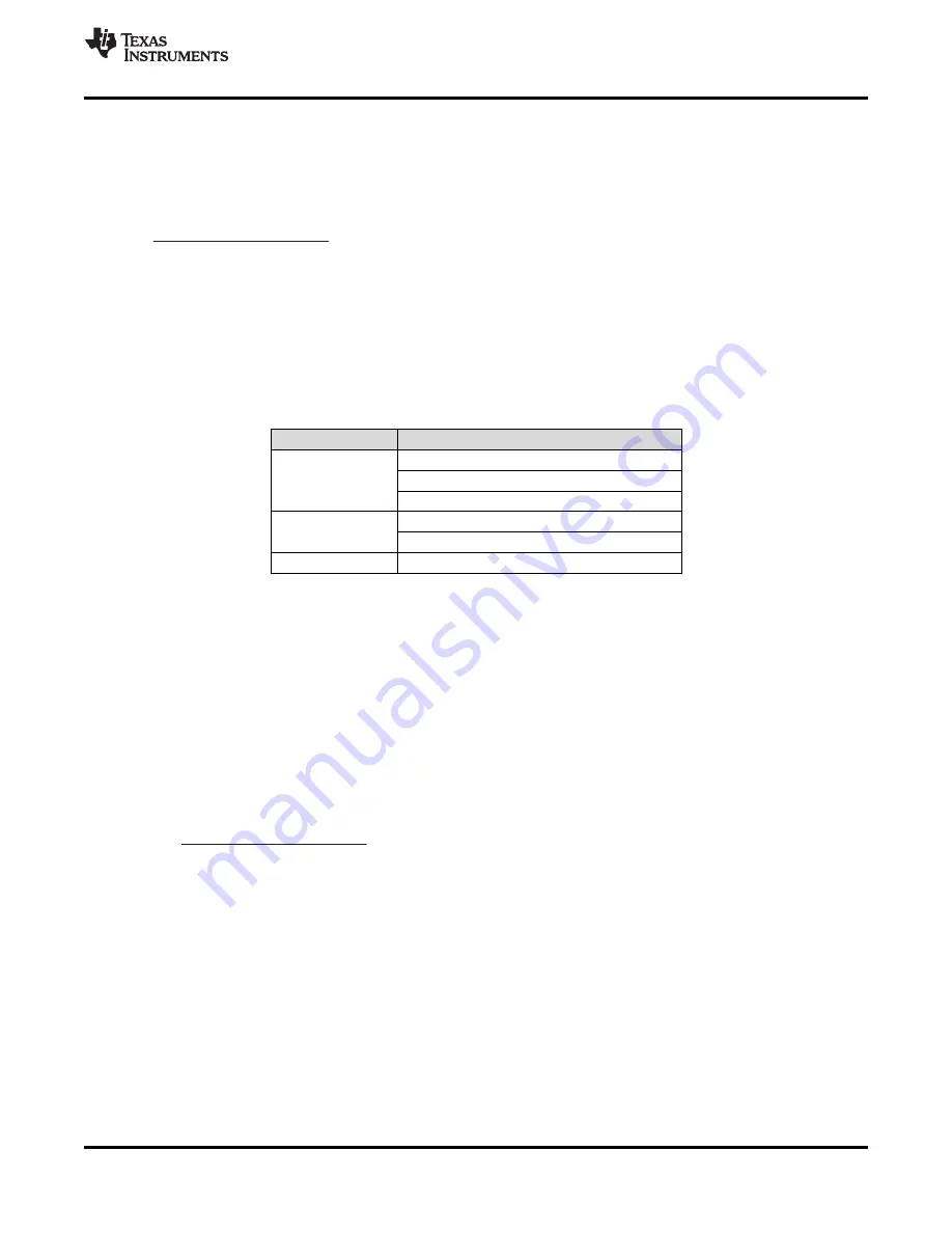
Table 4. List of Inductors

VENDOR

INDUCTOR SERIES

CDRH6D28

Sumida

CDRH6D38

CDRH103R

Wurth Elektronik

WE-PD type L

WE-PD type XL

EPCOS

B82464G

10.2.1.2.4

Capacitor Selection

10.2.1.2.4.1

Input Capacitor

At least a 10-µF input capacitor is recommended to improve transient behavior of the regulator and EMI behavior
of the total power supply circuit. A ceramic capacitor or a tantalum capacitor with a 100-nF ceramic capacitor in
parallel, placed close to the IC, is recommended.

10.2.1.2.4.2

Output Capacitor DC-DC Converter

The major parameter necessary to define the minimum value of the output capacitor is the maximum allowed
output voltage ripple in steady state operation of the converter. This ripple is determined by two parameters of
the capacitor, the capacitance and the ESR. It is possible to calculate the minimum capacitance needed for the
defined ripple, supposing that the ESR is zero, by using equation

Equation 6

:

(6)

Parameter

f

is the switching frequency and

Δ

V is the maximum allowed ripple.

With a chosen ripple voltage of 10 mV, a minimum capacitance of 53 µF is needed. The total ripple is larger due
to the ESR of the output capacitor. This additional component of the ripple can be calculated using

Equation 7

:

(7)

An additional ripple of 40 mV is the result of using a tantalum capacitor with a low ESR of 80 m

. The total ripple

is the sum of the ripple caused by the capacitance and the ripple caused by the ESR of the capacitor. In this
example, the total ripple is 50 mV. Additional ripple is caused by load transients. This means that the output
capacitance needs to be larger than calculated above to meet the total ripple requirements. The output capacitor
has to completely supply the load during the charging phase of the inductor. A reasonable value of the output
capacitance depends on the speed of the load transients and the load current during the load change. With the
calculated minimum value of 53 µF and load transient considerations, a reasonable output capacitance value is
in a 100 µF range. For economical reasons this usually is a tantalum capacitor. Because of this the control loop
has been optimized for using output capacitors with an ESR of above 30 m

.

Copyright © 2003–2014, Texas Instruments Incorporated

Submit Documentation Feedback

15

Product Folder Links:

TPS61090 TPS61091 TPS61092

Summary of Contents for TPS61090

Page 1: ...requency pulse width modulation PWM controller Low Battery Comparator using a synchronous rectifier to obtain maximum Low EMI Converter Integrated Antiringing Switch efficiency Boost switch and rectifier switch are Load Disconnect During Shutdown connected internally to provide the lowest leakage inductance and best EMI behavior possible The Over Temperature Protection maximum peak current in the ...

Page 2: ...lectrical Characteristics 4 13 2 Related Links 21 7 5 Typical Characteristics 6 13 3 Trademarks 21 8 Parameter Measurement Information 9 13 4 Electrostatic Discharge Caution 21 9 Detailed Description 10 13 5 Glossary 21 9 1 Overview 10 14 Mechanical Packaging and Orderable 9 2 Functional Block Diagram 10 Information 21 9 3 Feature Description 11 4 Revision History Changes from Revision B April 200...

Page 3: ...Package 10 Pins Top View Pin Functions PIN I O DESCRIPTION NAME NO EN 11 I Enable input 1 VBAT enabled 0 GND disabled FB 14 I Voltage feedback of adjustable versions GND 13 I O Control logic ground LBI 9 I Low battery comparator input comparator enabled with EN LBO 12 O Low battery comparator output open drain NC 2 Not connected PGND 5 6 7 I O Power ground PowerPAD Must be soldered to achieve appr...

Page 4: ...s XXX V may actually have higher performance 2 JEDEC document JEP157 states that 250 V CDM allows safe manufacturing with a standard ESD control process Manufacturing with less than 250 V CDM is possible with the necessary precautions Pins listed as YYY V may actually have higher performance 7 3 Recommended Operating Conditions MIN NOM MAX UNIT VI Supply voltage at VBAT 1 8 5 5 V L Inductance 2 2 ...

Page 5: ... V VBAT 2 4 V 0 1 1 CONTROL STAGE VUVL Under voltage lockout threshold VLBI voltage decreasing 1 5 V O VIL LBI voltage threshold VLBI voltage decreasing 490 500 510 mV LBI input hysteresis 10 LBI input current EN VBAT or GND 0 01 0 1 µA LBO output low voltage VO 3 3 V IOI 100 µA 0 04 0 4 V LBO output low current 100 µA LBO output leakage current VLBO 7 V 0 01 0 1 VIL EN SYNC input low voltage 0 2 ...

Page 6: ...3 V VI 1 8 V 2 4 V VSYNC 0 V Figure 4 Efficiency vs Output current TPS61092 VO 5 0 V VI 2 4 V 3 3 V VSYNC 0 V Figure 5 vs Output current TPS61091 IO 10 mA 100 mA 500 mA VSYNC 0 V Figure 6 vs Output current TPS61092 IO 10 mA 100 mA 500 mA VSYNC 0 V Figure 7 vs Output current TPS61091 VI 2 4 V Figure 8 Output voltage vs Output current TPS61092 VI 3 3 V Figure 9 No load supply current into VBAT Volta...

Page 7: ...4 V VI 3 3 V VO 5 V Efficiency IO Output Current mA 50 80 90 100 Efficiency VI Input Voltage V IO 10 mA IO 100 mA 1 8 2 2 6 2 8 3 2 2 2 4 3 2 60 IO 500 mA 70 V 5 V O TPS61090 TPS61091 TPS61092 www ti com SLVS484C JUNE 2003 REVISED DECEMBER 2014 Figure 5 TPS61092 Efficiency vs Output Current Figure 6 TPS61091 Efficiency vs Output Current Figure 8 TPS61091 Efficiency vs Output Current Figure 7 TPS61...

Page 8: ...ad resistance at Startup VI Input Voltage V TPS61090 TPS61091 TPS61092 SLVS484C JUNE 2003 REVISED DECEMBER 2014 www ti com Figure 11 TPS61092 No Load Supply Current Into VOUT vs Figure 12 Minimum Load Resistance at Start Up vs Input Input Voltage Voltage 8 Submit Documentation Feedback Copyright 2003 2014 Texas Instruments Incorporated Product Folder Links TPS61090 TPS61091 TPS61092 ...

Page 9: ...R8 C1 C2 X7R X5R Ceramic C3 Low ESR Tantalum VOUT Boost Output Low Battery Output R3 R4 R5 TPS61090 TPS61091 TPS61092 www ti com SLVS484C JUNE 2003 REVISED DECEMBER 2014 8 Parameter Measurement Information Figure 13 Parameter Schematic Copyright 2003 2014 Texas Instruments Incorporated Submit Documentation Feedback 9 Product Folder Links TPS61090 TPS61091 TPS61092 ...

Page 10: ...nverter to operate at a fixed switching frequency The TPS6109x family is based on a fixed frequency with multiple feed forward controller topology Input voltage output voltage and voltage drop on the NMOS switch are monitored and forwarded to the regulator The peak current of the NMOS switch is also sensed to limit the maximum current flowing through the switch and the inductor It can also operate...

Page 11: ...t is compared with the internal reference voltage to generate an accurate and stable output voltage The peak current of the NMOS switch is also sensed to limit the maximum current flowing through the switch and the inductor The typical peak current limit is set to 2200 mA An internal temperature sensor prevents the device from getting overheated in case of excessive power dissipation 9 3 3 Device ...

Page 12: ...ove the threshold It is active low when the voltage at LBI goes below 500 mV The battery voltage at which the detection circuit switches can be programmed with a resistive divider connected to the LBI pin The resistive divider scales down the battery voltage to a voltage level of 500 mV which is then compared to the LBI threshold voltage The LBI pin has a built in hysteresis of 10 mV See the appli...

Page 13: ...TPS6109x converter operates with the nominal switching frequency of 600 kHz As the load current decreases the converter enters power save mode reducing the switching frequency and minimizing the IC quiescent current to achieve high efficiency over the entire load current range The power save mode can be disabled by setting the SYNC to VBAT TPS6109x converter always operates with the nominal switch...

Page 14: ...be easily calculated using Equation 2 2 10 2 1 2 2 Programming the LBI LBO Threshold Voltage The current through the resistive divider should be about 100 times greater than the current into the LBI pin The typical current into the LBI pin is 0 01 µA and the voltage across R2 is equal to the LBI voltage threshold that is generated on chip which has a value of 500 mV The recommended value for R2is ...

Page 15: ...100 nF ceramic capacitor in parallel placed close to the IC is recommended 10 2 1 2 4 2 Output Capacitor DC DC Converter The major parameter necessary to define the minimum value of the output capacitor is the maximum allowed output voltage ripple in steady state operation of the converter This ripple is determined by two parameters of the capacitor the capacitance and the ESR It is possible to ca...

Page 16: ...1 2 4 3 Small Signal Stability When using output capacitors with lower ESR like ceramics it is recommended to use the adjustable voltage version The missing ESR can be easily compensated there in the feedback divider Typically a capacitor in the range of 10 pF in parallel to R3 helps to obtain small signal stability with lowest ESR output capacitors For more detailed analysis the small signal tran...

Page 17: ...TPS6109xRSA L1 Sumida CDRH103R 6R8 C1 C2 X7R X5R Ceramic C3 Low ESR Tantalum VCC 5 V Boost Output LBO R5 Battery Input TPS61090 TPS61091 TPS61092 www ti com SLVS484C JUNE 2003 REVISED DECEMBER 2014 10 2 2 TPS6109x Application Schematic of 5 Vout With Maximum Output Power Figure 20 Power Supply Solution for Maximum Output Power Schematic 10 2 3 TPS6109x Application Schematic of 5 Vout and Auxiliary...

Page 18: ...nregulated Auxiliary Output Battery Input FB VCC1 5 V Boost Main Output TPS61090 TPS61091 TPS61092 SLVS484C JUNE 2003 REVISED DECEMBER 2014 www ti com 10 2 4 TPS6109x Application Schematic of 5 Vout and Auxiliary 5 Vout With Charge Pump Figure 22 Power Supply Solution With Auxiliary Negative Output Voltage Schematic 18 Submit Documentation Feedback Copyright 2003 2014 Texas Instruments Incorporate...

Page 19: ...ally at high peak currents and high switching frequencies If the layout is not carefully done the regulator could show stability problems as well as EMI problems Therefore use wide and short traces for the main current path and for the power ground tracks The input capacitor output capacitor and the inductor should be placed as close as possible to the IC Use a common ground node for power ground ...

Page 20: ...B design Improving the thermal coupling of the component to the PCB Introducing airflow in the system The maximum junction temperature TJ of the TPS6109x devices is 150 C The thermal resistance of the 16 pin QFN PowerPAD package RSA isRΘJA 38 1 C W if the PowerPAD is soldered and the board layout is optimized Specified regulator operation is assured to a maximum ambient temperature TA of 85 C Ther...

Page 21: ...ere Click here Click here Click here TPS61092 Click here Click here Click here Click here Click here 13 3 Trademarks PowerPAD is a trademark of Texas Instruments All other trademarks are the property of their respective owners 13 4 Electrostatic Discharge Caution These devices have limited built in ESD protection The leads should be shorted together or the device placed in conductive foam during s...

Page 22: ...Width W1 mm A0 mm B0 mm K0 mm P1 mm W mm Pin1 Quadrant TPS61090RSAR QFN RSA 16 3000 330 0 12 4 4 3 4 3 1 5 8 0 12 0 Q2 TPS61091RSAR QFN RSA 16 3000 330 0 12 4 4 3 4 3 1 5 8 0 12 0 Q2 TPS61092RSAR QFN RSA 16 3000 330 0 12 4 4 3 4 3 1 5 8 0 12 0 Q2 PACKAGE MATERIALS INFORMATION www ti com 25 Dec 2014 Pack Materials Page 1 ...

Page 23: ...Drawing Pins SPQ Length mm Width mm Height mm TPS61090RSAR QFN RSA 16 3000 338 1 338 1 20 6 TPS61091RSAR QFN RSA 16 3000 338 1 338 1 20 6 TPS61092RSAR QFN RSA 16 3000 338 1 338 1 20 6 PACKAGE MATERIALS INFORMATION www ti com 25 Dec 2014 Pack Materials Page 2 ...

Page 24: ......

Page 25: ......

Page 26: ......

Page 27: ...esponsible for compliance with all legal regulatory and safety related requirements concerning its products and any use of TI components in its applications notwithstanding any applications related information or support that may be provided by TI Buyer represents and agrees that it has all the necessary expertise to create and implement safeguards which anticipate dangerous consequences of failur...

Reviews: