background image

www.ti.com

General Configurations

fully turned off when VIN2 (TP15) reaches 2.1 V (+0.3 V). Verify that the PG2 green LED (D7) turns off
and the FLTb2 red LED (D6) turns ON.

3. Increase the input voltage on VIN2 and monitor VOUT2. Verify that VOUT2 (TP16) starts increasing

and is fully turned off when VIN2 (TP15) reaches 15.5 V (±1 V). Verify that the PG2 green LED (D7)
turns off and the FLTb2 red LED (D6) turns ON.

4. Turn off the power supply.

4.4.1.3

Ramp-Up Time Test (CH1 and CH2)

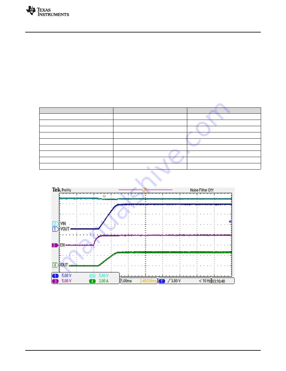
1. Verify ramp-up time (CH1 and CH2, with only 1 channel powered at a time). Set up the oscilloscope as

shown in

Table 7

.

Table 7. PWR635 Oscilloscope Setting for Ramp-Up Voltage Test

Oscilloscope Setting

CH1 Probe Points

CH2 Probe Points

Channel 1 = 5 V/div

TP2 = VOUT1

TP16 = VOUT2

Channel 2 = 5 V/div

TP3 = VIN1

TP15 = VIN2

Channel 3 = 5 V/div

TP8 = EN/UVLO1

TP17 = EN/UVLO2

Channel 4 = 2 A/div

Current probe in input +Ve wire

Current probe in input +Ve wire

Trigger source = Channel 1

Trigger level = 6.0 ±0.5 V

Trigger polarity = Positive

Trigger Mode = Single Sequence

Time base = 1 ms/div

2. Set the output load at 5

Ω

on CH1 and then enable the load. Turn on the power supply, Press the EVM

RST switch (S1) and release, verify that VOUT1 (TP2) ramps up as shown in

Figure 3

.

Figure 3. Vout Ramp-Up Time of Auto-Retry Circuit Breaker (CH1)

3. Set the output load at 5

Ω

on CH2 and then enable the load. Turn on the power supply, Press the EVM

RST switch (S2) and release, verify that VOUT2 (TP16) ramps up as shown in

Figure 4

.

9

SLUUBC2A – May 2015 – Revised July 2015

TPS25944X635EVM: Evaluation Module for TPS25944X

Submit Documentation Feedback

Copyright © 2015, Texas Instruments Incorporated

Summary of Contents for TPS25944X635EVM

Page 1: ...with TPS25944A 3 Replace the U2 as the with TPS25944L 4 Make sure the following parts are unpopulated R7 R8 Contents 1 Introduction 2 1 1 EVM Features 2 1 2 EVM Applications 2 2 Description 3 3 Schem...

Page 2: ...18 0 V TYP operation CH1 rising input voltage turn On threshold 10 8 V TYP CH1 falling input voltage turn off threshold 10 V TYP CH2 rising input voltage turn On threshold 10 8 V TYP CH2 falling input...

Page 3: ...otection S1 allows U1 and S2 allows U2 to be RESET or disabled A power good PG indicator is provided by D2 and D6 for CH1 and CH2 respectively and circuit faults can be observed with D2 and D6 Scaled...

Page 4: ...R16 100k R17 20V D8 B320A 13 F 20V D4 B320A 13 F 330 F C10 16V D9 16V D5 4 7 F C2 4 7 F C3 4 7 F C8 4 7 F C9 DEVSLP 1 PGOOD 2 PGTH 3 OUT 4 OUT 5 OUT 6 OUT 7 OUT 8 IN 9 IN 10 IN 11 IN 12 IN 13 EN UVLO...

Page 5: ...supply to the EVM TP17 EN_UV2 CH2 Active high enable and under voltage input TP18 OVP2 CH2 Active high overvoltage input TP22 IMON2 CH2 Current monitor Load current 1 187 voltage on TP22 TP16 VOUT2 CH...

Page 6: ...us measurements are needed 4 2 3 Oscilloscope A DPO2024 or Lecroy 424 oscilloscope or equivalent three 10X voltage probes and a DC current probe 4 2 4 Loads One resistive load or equivalent which take...

Page 7: ...P A L P H A S H I F T E N T E R R U N DG ER F I AJ BK C L 7M 8N 9O DG DG DG DG T 3U 0V W X Y Z T A B U T I L I Z A T I O N H U B M A U N I C 2 B N C 4 M b s Oscilloscope xx xx xx xx x x xx xx x x Texa...

Page 8: ...3 0 1 VDC EN_UV2 TP17 12 0 3 VDC OVP1 TP5 0 742 0 1 VDC OVP2 TP18 0 742 0 1 VDC IMON1 TP11 33 8 mV 5 mVDC IMON2 TP22 33 8 mV 5 mVDC VOUT1 TP2 12 0 3 VDC VOUT2 TP16 12 0 3 VDC PG1 TP9 2 40 0 1 VDC PG2...

Page 9: ...nel 1 5 V div TP2 VOUT1 TP16 VOUT2 Channel 2 5 V div TP3 VIN1 TP15 VIN2 Channel 3 5 V div TP8 EN UVLO1 TP17 EN UVLO2 Channel 4 2 A div Current probe in input Ve wire Current probe in input Ve wire Tri...

Page 10: ...l 4 5 A div Input current into J3 Ve wire Input current into J8 Ve wire Trigger source Channel 4 Trigger level 1 0 0 2 A Trigger polarity Ve Trigger Mode Single Sequence Time base 40 ms div 1 If an el...

Page 11: ...4 36 ms Figure 5 Output Short Circuit Behavior of Auto Retry Circuit Breaker CH1 Figure 6 Circuit Breaking Time Delay CH1 4 Set the output load at 1 0 0 1 on CH1 and current limit to 5 3 A and then en...

Page 12: ...ker CH2 Figure 8 Circuit Breaking Time Delay CH2 5 Set the input power supply to zero volts and disconnect all equipment from the DUT 12 TPS25944X635EVM Evaluation Module for TPS25944X SLUUBC2A May 20...

Page 13: ...Drawings Figure 9 through Figure 11 show component placement and layout of the EVM Figure 9 Top Side Placement Figure 10 Top Side Routing Layer 13 SLUUBC2A May 2015 Revised July 2015 TPS25944X635EVM...

Page 14: ...ayout Guidelines www ti com Figure 11 Bottom Side Routing Layer 14 TPS25944X635EVM Evaluation Module for TPS25944X SLUUBC2A May 2015 Revised July 2015 Submit Documentation Feedback Copyright 2015 Texa...

Page 15: ...Any LBL1 1 Thermal Transfer Printable Labels 0 650 W x 0 200 H 10 000 per PCB Label 0 650 H x THT 14 423 10 Brady roll 0 200 W Q1 1 30V MOSFET N CH 30V 100A SON 5x6mm SON 5x6mm CSD17301Q5A Texas Instr...

Page 16: ...nt Any TP26 TP12 TP13 4 SMT Test Point SMT Compact Testpoint_Keystone_Com 5016 Keystone Equivalent Any TP24 TP25 pact U1 1 2 7V 18V eFuse with True Reverse Blocking for Power Mux RVC0020A TPS25944ARVC...

Page 17: ...ision Page Added Important Note to TPS25944XEVM 635 Users 1 NOTE Page numbers for previous revisions may differ from page numbers in the current version 17 SLUUBC2A May 2015 Revised July 2015 Revision...

Page 18: ...ing the warranty period to the address designated by TI and that are determined by TI not to conform to such warranty If TI elects to repair or replace such EVM TI shall have a reasonable time to repa...

Page 19: ...transmitter has been approved by Industry Canada to operate with the antenna types listed in the user guide with the maximum permissible gain and required antenna impedance for each antenna type indic...

Page 20: ...ified allowable ranges some circuit components may have elevated case temperatures These components include but are not limited to linear regulators switching transistors pass transistors current sens...

Page 21: ...REMOVAL OR REINSTALLATION ANCILLARY COSTS TO THE PROCUREMENT OF SUBSTITUTE GOODS OR SERVICES RETESTING OUTSIDE COMPUTER TIME LABOR COSTS LOSS OF GOODWILL LOSS OF PROFITS LOSS OF SAVINGS LOSS OF USE L...

Page 22: ...sponsible for compliance with all legal regulatory and safety related requirements concerning its products and any use of TI components in its applications notwithstanding any applications related inf...

Reviews: