


Test Point
Headers
TP1 to
TP4
10-Pin
SM-DIG Connector
I C Interface
2
TMP102
J1
4
TMP102EVM Hardware Setup
2.1
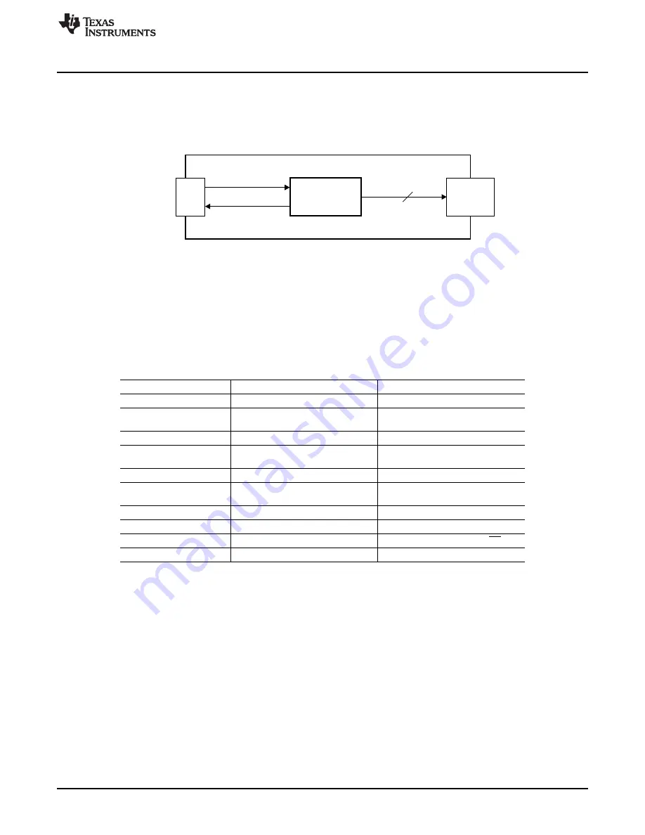
Theory of Operation for TMP102 Hardware
The TMP102EVM only requires the two-wire I
2
C lines (SDA and SCLK) and V
DUT
/GND to supply a
constant 3.3 V and power return, as shown in
. The TMP102EVM also has test points to monitor
these signal lines and ground, in case users may want to use their own signals or verify successful I
2
C
communications.
Figure 3. TMP102EVM Board Block Diagram
2.2
Signal Definitions of H1 (10-Pin Male Connector Socket)
shows the pinout for the 10-pin connector socket used to communicate between the TMP102EVM
and the SM-USB-DIG. It should be noted that the TMP102EVM uses only the necessary I
2
C
communication lines (pins 1 and 3) and the V
DUT
and GND (pins 6 and 8, respectively) to issue commands
to the TMP102 sensors.
Table 3. Signal Definition of H1 on TMP102EVM Board
Pin on U1
Signal
Description
1
I2C_SCL
I
2
C Clock Signal (SCL)
2
CTRL/MEAS4
GPIO: Control Output or Measure
Input
3
I2C_SDA1
I
2
C Data Signal (SDA)
4
CTRL/MEAS5
GPIO: Control Output or Measure
Input
5
SPI_DOUT1
SPI Data Output (MOSI)
6
V
DUT
Switchable DUT Power Supply: +3.3
V, +5 V, Hi-Z (Disconnected)
(1)
7
SPI_CLK
SPI Clock Signal (SCLK)
8
GND
Power Return (GND)
9
SPI_CS1
SPI Chip Select Signal (CS)
10
SPI_DIN1
SPI Data Input (MISO)
(1)
When V
DUT
is Hi-Z, all digital I/O are Hi-Z as well.
5
SBOU114
–
August 2011
TMP102EVM Evaluation Board and Software Tutorial
Copyright
©
2011, Texas Instruments Incorporated