


PRODUCTPREVIEW
EQEP1A
VIM
EQEP1INTn
EQEP1
Module
IO
Mux
EQEP1ENCLK
EQEP1IO
EQEP1I
VBus32
VCLK4
SYS_nRST
EQEP1B
EQEP1IOE
EQEP1SO
EQEP1S
EQEP1SOE
EQEP1ERR
EPWM1/../7
TZ4n
EQEP2A
VIM
EQEP2INTn
EQEP2
Module
EQEP2ENCLK
EQEP2IO
EQEP2I
VBus32
VCLK4
SYS_nRST
EQEP2B
EQEP2IOE
EQEP2SO
EQEP2S
EQEP2SOE
EQEP2ERR
Connection
Selection
Mux
RM46L852
SPNS185 – SEPTEMBER 2012
5.3
Enhanced Quadrature Encoder (eQEP)
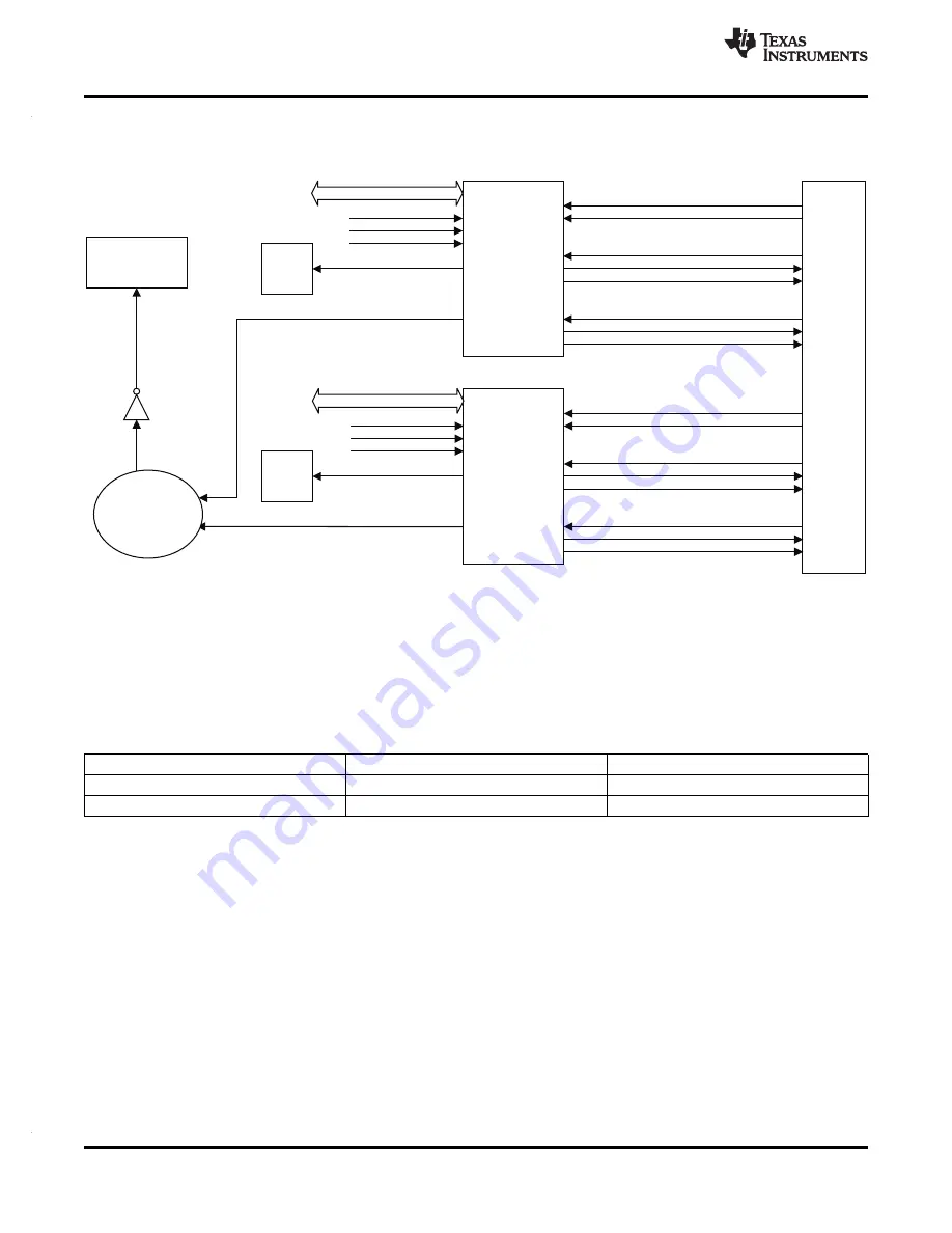
shows the eQEP module interconnections on the device.
Figure 5-4. eQEP Module Interconnections
5.3.1
Clock Enable Control for eQEPx Modules
Device-level control registers are implemented to generate the EQEPxENCLK signals. When SYS_nRST
is active low, the clock enables are ignored and the eQEPx logic is clocked so that it can reset to a proper
state. When SYS_nRST goes in-active high, the state of clock enable is respected.
Table 5-11. eQEPx Clock Enable Control
ePWM Module Instance
Control Register to Enable Clock
Default Value
eQEP1
PINMMR40[16]
1
eQEP2
PINMMR40[24]
1
The default value of the control registers to enable the clocks to the eQEPx modules is 1. This means that
the VCLK4 clock connections to the eQEPx modules are enabled by default. The application can choose
to gate off the VCLK4 clock to any eQEPx module individually by clearing the respective control register
bit.
5.3.2
Using eQEPx Phase Error to Trip ePWMx Outputs
The eQEP module sets the EQEPERR signal output whenever a phase error is detected in its inputs
EQEPxA and EQEPxB. This error signal from both the eQEP modules is input to the connection selection
multiplexor. This multiplexor is defined in
. As shown in
, the output of this selection
multiplexor is inverted and connected to the TZ4n trip-zone input of all EPWMx modules. This connection
allows the application to define the response of each ePWMx module on a phase error indicated by the
eQEP modules.
124
Peripheral Information and Electrical Specifications
Copyright © 2012, Texas Instruments Incorporated
Summary of Contents for RM46L852
Page 170: ......


