Valid Address
D0
D1
D2
D3
OUT
IN
OUT
CSONTIME
ADVONTIME
ADVRDOFFTIME
OEONTIME
OEOFFTIME0
CLKACTIVATIONTIME
CSRDOFFTIME0
RDACCESSTIME
RDCYCLETIME0
PAGEBURSTACCESSTIME
PAGEBURSTACCESSTIME
PAGEBURSTACCESSTIME
RDCYCLETIME1
CSRDOFFTIME1
OEOFFTIME1
GPMC_FCLK
GPMC_CLK
gpmc_a[11:1]
gpmc_d[15:0]
nBE1/nBE0
nCS
nADV
nOE
DIR
WAIT
(connected to A [9:0] on memory side)
(connected to D [15:0] on memory side)
gpmc-019
Valid Address
Public Version
General-Purpose Memory Controller
www.ti.com
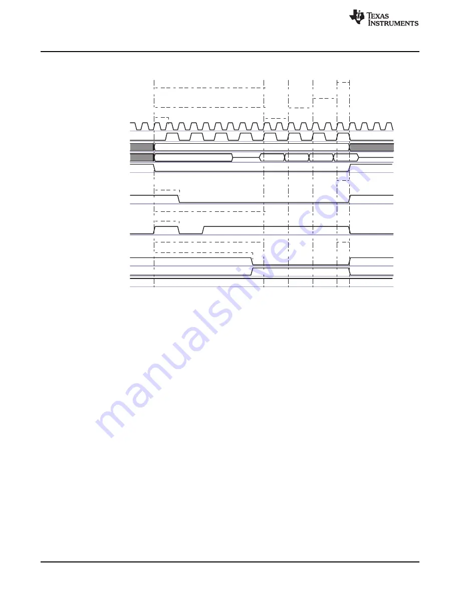
Figure 10-19. Synchronous Multiple (Burst) Read (GPMCFCLKDIVIDER = 1)
NOTE: The WAIT signal is active low.
In the following section i stands for the chip-select number, i = 0 to 7.
•
GPMC.
register settings:
–
READMULTIPLE bit at 1 (read multiple access)
–
READTYPE bit at 1 (read synchronous)
–
MUXADDDATA bit at 0 (nonaddress/data-multiplexed device)
When RDACCESSTIME completes, control-signal timings are frozen during the multiple data transactions,
corresponding to PAGEBURSTACCESSTIME multiplied by the number of remaining data transactions.
•
Chip-select signal nCS:
–
nCS assertion time is controlled by the GPMC.
[3:0] CSONTIME field and
ensures address setup time to nCS assertion.
–
nCS deassertion time is controlled by the GPMC.
[12:8] CSRDOFFTIME field
and ensures address hold time to nCS deassertion.
•
Address valid signal nADV:
–
nADV assertion time is controlled by the GPMC.
[3:0] ADVONTIME field.
–
nADV deassertion time is controlled by the GPMC.
[12:8] ADVRDOFFTIME
field.
•
Output enable signal nOE:
–
nOE assertion indicates a read cycle.
–
nOE assertion time is controlled by the GPMC.
[3:0] OEONTIME field.
–
nOE deassertion time is controlled by the GPMC.
[12:8] OEOFFTIME field.
•
Initial latency for the first read data is controlled by GPMC.
[20:16]
RDACCESSTIME or by monitoring the WAIT signal.
•
Successive read data are provided by the memory device each one or two GPMC_CLK cycles. The
PAGEBURSTACCESSTIME parameter must be set accordingly with GPMCFCLKDIVIDER and the
memory-device internal configuration.
2152
Memory Subsystem
SWPU177N – December 2009 – Revised November 2010
Copyright © 2009–2010, Texas Instruments Incorporated


