ESD Protection
R
100
»
W
ADC12MCTLx.0–3
Input
Ax
ADC12_B Operation
872
SLAU367P – October 2012 – Revised April 2020
Copyright © 2012–2020, Texas Instruments Incorporated
ADC12_B
34.2.2 ADC12_B Inputs and Multiplexer
Up to 32 external and up to 6 internal analog signals are selected as the channel for conversion by the
analog input multiplexer based on the ADC12INCHx bit and for A
26
- A
31
the ADC12CTL3 register. The
number of channels that are available as well as internal channel 0-3 is device specific and is shown in
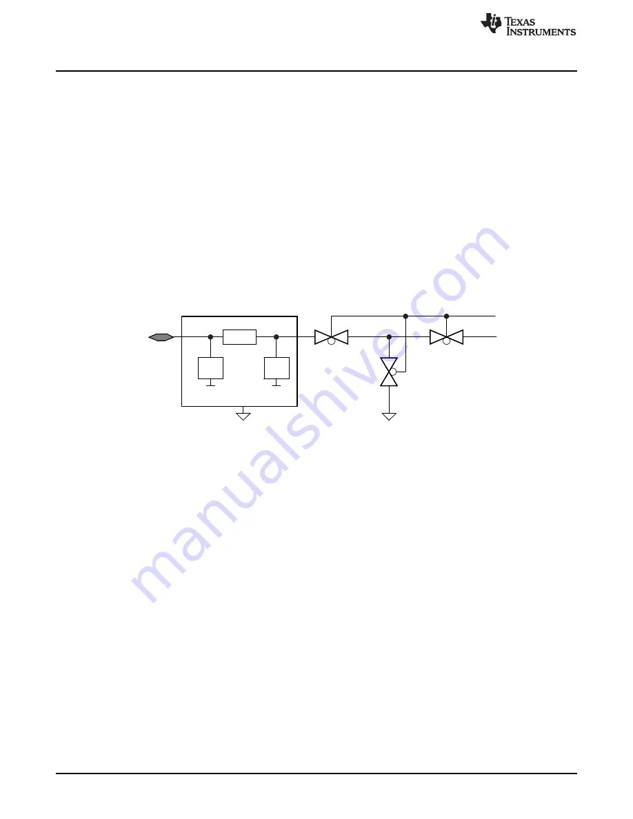
the device-specific data sheet. The input multiplexer is a break-before-make type to reduce input-to-input
noise injection that can result from channel switching (see
). The input multiplexer is also a T-
switch to minimize the coupling between channels. Channels that are not selected are isolated from the
ADC, and the intermediate node is connected to analog ground (AVSS), so that the stray capacitance is
grounded to eliminate crosstalk.
The ADC12_B supports single-ended input or differential inputs configurable for each conversion memory
with the ADC12DIF bit in the ADC12_B Conversion Memory Control x Register (ADC12MCTLx).
Differential input mode should be selected for differential input signals and can also be used for single-
ended signals by tying the negative input to AVSS. The advantage of using differential mode is increased
common mode noise rejection at the cost of a small increase in current consumption.
The ADC12_B uses the charge redistribution method. When the inputs are internally switched, the
switching action may cause transients on the input signal. These transients decay and settle before
causing errant conversion.
Figure 34-2. Analog Multiplexer T-Switch
34.2.2.1 Analog Port Selection
The ADC12_B inputs are multiplexed with digital port pins. When analog signals are applied to digital
gates, parasitic current can flow from V
CC
to GND. This parasitic current occurs if the input voltage is near
the transition level of the gate. Disabling the digital part of the port pin eliminates the parasitic current flow
and, therefore, reduces overall current consumption. The PySELx bits can disable the port pin input and
output buffers. Refer to the device specific port x input/output schematic and table for the ADC12_B input
pin for PySELx details.
34.2.3 Voltage References
The ADC12_B module may use an on-chip shared reference module that supplies three selectable
voltage levels of 1.2 V, 2.0 V, and 2.5 V (see the reference module for proper configuration details) to
supply V
R+
and V
R-
. These reference voltages may be used internally and externally on pin VREF+ if
REFOUT=1. Alternatively, external references may be supplied for V
R+
and V
R-
through pins
VREF+/VeREF+ and VeREF-. The ADC12_B module reference selection is through the ADC12VRSEL
bits. For pin flexibility VR+ and VR- are not restricted to VeREF+ and VeREF- respectively. Care must be
taken that ADC12VRSEL does not conflict with REFOUT bit settings as only one buffer is available for
internal reference with REFOUT=1 or ADC12_B module reference when external reference with internal
buffer is selected . So if REFOUT=1, VeREF+ buffered should not be selected with ADC12VRSEL = 0x3,
0x5, or 0xF.


