2 Input, Output Voltages, and Load Current Requirements
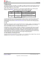
LP87745-Q1 device works with 3.3 V input supply and supply is internally monitored for undervoltage (UV) and
overvoltage (OV) conditions and hence keep the input supply voltage within 3.3 V +/- 6 % to avoid input supply
UV/OV detection.
• If the VBAT/pre-regulator path is used (default configuration), input supply to the device is already regulated
to 3.3 V.
• If external 3.3 V supply is used, ensure that input supply voltage is always within the recommended voltage
range and drop across supply path must be considered.
• If EVM is configured to work with USB supply, regulators should not be loaded.
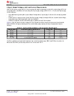
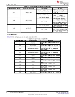
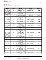
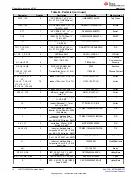
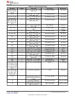
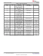
lists the input and output voltage for each regulator and their maximum load-current requirements.
Refer LP87745-Q1 device data sheet for more information about device electrical characteristics and its
features.
Table 2-1. Input and Output Voltages, and Load Current Requirements
Regulator Name
Input Supply Voltage at PMIC Supply Pin
Output Voltage
Maximum Load Current
BUCK1
3.1 V - 3.5 V
1.8 V
3 A
BUCK2
3.1 V - 3.5 V
1.0 V
3 A
BUCK3
3.1 V - 3.5 V
1.2 V
3 A
BOOST
3.1 V - 3.5 V
5 V
0.3 A
VIO_LDO
5 V (Generated from BOOST)
3.3 V
0.150 A
If all the regulators are loaded with maximum load current simultaneously, PMIC and PCB can become hot.
Make sure that PMIC junction temperature does not exceed 150 °C.
Input, Output Voltages, and Load Current Requirements
LP877451Q1EVM Evaluation Module
3
Copyright © 2021 Texas Instruments Incorporated


