background image

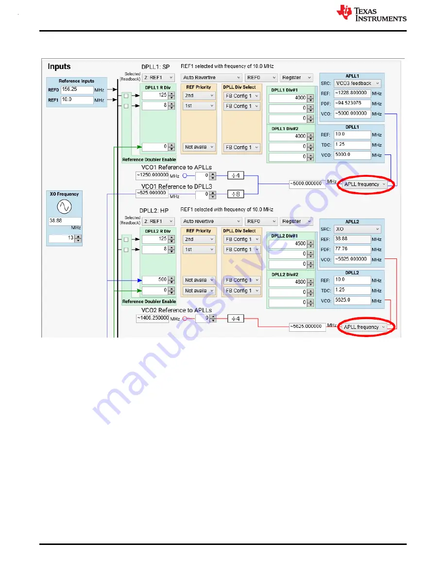
On this page, it is possible to select the APLL frequency or DPLL frequency to propagate through to the outputs
by changing APLL frequency to DPLL frequency.

Figure 6-9. APLL or DPLL Frequency Selection

Appendix A - TICS Pro LMK5C33216 Software

www.ti.com

AD
V

A

NCE INFO

R

MA
TION

32

LMK5C33216EVM User's Guide

SNAU260A – OCTOBER 2020 – REVISED FEBRUARY 2021

Submit Document Feedback

Copyright © 2021 Texas Instruments Incorporated

Summary of Contents for LMK5C33216EVM

Page 1: ...s IN0 to IN1 Schematic 16 4 4 Clock Outputs OUT0 to OUT3 Schematic 17 4 5 Clock Outputs OUT4 to OUT9 Schematic 18 4 6 Clock Outputs OUT10 to OUT15 Schematic 19 4 7 XO Schematic 20 4 8 Logic I O Interfaces Schematic 21 4 9 USB2ANY Schematic 22 5 EVM Bill of Materials 23 5 1 Loop Filter and Vibration Nonsensitive Capacitors 27 6 Appendix A TICS Pro LMK5C33216 Software 28 6 1 Using the Start Page 28 ...

Page 2: ...d through the onboard USB microcontroller MCU interface using a PC with TI s TICS Pro software graphical user interface GUI TICS Pro can be used to program the LMK5C33216 registers Features LMK5C33216 DUT What is Included LMK5C33216EVM What is Needed Windows PC with TICS Pro Software GUI Test Equipment DC power supply 5 V 2 A Real time oscilloscope Source signal analyzer Precision frequency counte...

Page 3: ...fault Setting of Jumpers and Dip Switches www ti com Introduction ADVANCE INFORMATION SNAU260A OCTOBER 2020 REVISED FEBRUARY 2021 Submit Document Feedback LMK5C33216EVM User s Guide 3 Copyright 2021 Texas Instruments Incorporated ...

Page 4: ...ct references a 156 25 MHz reference clock to IN0_P N and or b 10 MHz reference clock to IN1_P N 4 Connect USB cable to USB port at J41 Software Setup 1 If not already installed install TICS Pro software from TI website 2 If the MATLAB R2015b 9 0 64 bit runtime is not already installed download and install from MathWorks website While optional for programming and evaluating the default profile set...

Page 5: ... consumption should be approximately 1 15 A 4 Check LMK5C33216 Status a Status Page of GUI b Click Read Status Bits c To clear latched bits i Press Clear Latched Bits button ii Read Status Bits d It may take some time for the DPLL status bits to reflect lock www ti com EVM Quick Start ADVANCE INFORMATION SNAU260A OCTOBER 2020 REVISED FEBRUARY 2021 Submit Document Feedback LMK5C33216EVM User s Guid...

Page 6: ...easurements may now be made at the clock outputs EVM Quick Start www ti com ADVANCE INFORMATION 6 LMK5C33216EVM User s Guide SNAU260A OCTOBER 2020 REVISED FEBRUARY 2021 Submit Document Feedback Copyright 2021 Texas Instruments Incorporated ...

Page 7: ...6 DUT 2 A J1 VIN1 terminal block header or External Supply 5 V using default configuration B J2 VIN1 SMA Not populated by default 3 A Y1 or B J8 4 J4 5 J6 7 SMA Ports for DUT Clock Inputs IN0_P N and IN1_P N 5 J9 11 J10 12 J13 15 J14 16 J17 19 J18 20 J21 J23 J22 24 J25 27 J26 28 J29 31 J30 32 J33 35 J34 36 J37 39 J38 40 SMA Ports for DUT Clock Outputs 6 S5 Normally open Push button for DUT power d...

Page 8: ...VM the default power configuration uses the onboard LDO regulators to power all VDD and VDDO pins from an external 5 V supply input VIN1 to J1 or J2 A Dual LDO regulator U3 is used to power the VDD and VDDO rails of the DUT and its peripheral circuitry A separate LDO regulator U4 also supplied from VIN1 is used to power the onboard XO circuits EVM Configuration www ti com ADVANCE INFORMATION 8 LMK...

Page 9: ...upply ground Pin 1 VIN1 Connect to external 3 3 V supply Pin 2 VIN2 Connect to external 3 3 V supply Pin 3 VIN3 n a Pin 4 GND Connect to supply ground JP1 VDD Tie pins 1 2 adjacent to designator to select 3 3 V from LDO1 to VDD Plane Tie pins 2 3 opposite to designator to select external VIN1 to VDD Plane JP2 VDDO Tie pins 1 2 adjacent to designator to select 3 3 V from LDO2 to VDDO Plane Tie pins...

Page 10: ...ice Start Up Modes GPIO1 Input Level1 Start up Mode 0 I2C Mode 1 SPI Mode 1 The input levels on these pins are sampled only during POR 3 3 Switching Between I2C and SPI To switch the EVM between I2C and SPI modes the switches and jumpers must be configured as follows Figure 3 3 I2C Mode Jumper Configuration Figure 3 4 SPI Mode Jumper Configuration In SPI mode GPIO2 must also be configured as STATU...

Page 11: ...F Request Control Figure 3 9 GPIO Pin Selection for SYSREF 3 5 XO Input The LMK5C33216 has an XO input XO_P pin to accept a reference clock for the Fractional N APLLs The XO input determines the output frequency accuracy and stability in free run or holdover modes For synchronization applications like SyncE or IEEE 1588 the XO input would typically be driven by a low frequency TCXO OCXO or externa...

Page 12: ...CXO footprints to be used By default Y1 is populated with a 38 88 MHz TCXO and selected with the populated R43 Other XO TCXO OCXO may be installed and connected using the appropriate resistor Care should be taken if more than one device is installed to remove resistors for isolation Figure 3 10 XO Input 3 5 1 38 88 MHz TCXO Default By default the EVM is populated with a 38 88 MHz 3 3 V LVCMOS low ...

Page 13: ... are AC coupled to the SMA ports labeled OUT 0 15 _P N 3 8 Status Outputs and LEDS Status outputs signals can be configured on the GPIO0 GPIO1 and GPIO2 pins The status output signal output type 3 3 V LVCMOS or NMOS open drain 3 9 Requirements for Making Measurements When performing measurements with the LMK5C33216EVM the following procedures must be completed 1 Ensure all required outputs have pr...

Page 14: ... PAD 9 U3 0 47uF C22 0 47uF C26 DUT VDDO OUTPUT POWER 3 3V LDO1 OUT 3 3 V LDO2 OUT 3 3 V 1 2 3 4 J1 PWR TP6 LDO3 DNP TPS7A8801RTJR IN1 1 IN1 2 GND 3 IN2 4 IN2 5 EN2 6 NR SS2 7 SS_CTRL2 8 PG2 9 FB2 10 OUT2 11 OUT2 12 GND 13 OUT1 14 OUT1 15 FB1 16 PG1 17 SS_CTRL1 18 NR SS1 19 EN1 20 PAD 21 U2 1 2 3 JP3 M20 8770342 LDO3 IN 1uF C5 VDD_PLANE TP2 VDD 10uF C4 1uF C6 22uF C3 DUT VDD CORE POWER 3 3V 1 2 3 ...

Page 15: ...1uF C58 0 1uF C55 10uF C56 FB10 TP8 VDD_IN0 DNP TP10 VDD_IN1 DNP TP12 VDD_DIG DNP TP14 VDD_APLL1_XO DNP TP16 VDD_APLL2 DNP TP18 VDD_APLL3 DNP VDD_PLANE VDDO_PLANE VCC_XO TP9 VDDO_01 DNP TP11 VDDO_23 DNP TP13 VDDO_4TO7 DNP TP15 VDDO_8TO13 DNP VDDO_1415 0 1uF C42 0 1uF C48 0 1uF C54 0 1uF C60 0 1uF C30 0 1uF C36 0 1uF C33 0 1uF C39 0 1uF C57 0 1uF C45 0 1uF C51 NT1 NT_0603 0 R11 0 R16 0 R18 0 R20 0 ...

Page 16: ...50 GPIO1 64 GPIO2 10 CAP1_APLL2 22 CAP2_APLL2 21 CAP3_APLL2 20 CAP_DIG 40 IN0_N 35 IN0_P 34 IN1_N 38 IN1_P 39 U1 EXT SMA XO CLK SMA_XO_P XO2_P 0 R41 1 2 3 4 5 J8 142 0701 201 49 9 R42 DNP XO1_P 0 1uF R40 0 1uF C70 0 1uF C71 25V 100nF C67 25V 0 047µF C68 DNP SMA_IN0_P SMA_IN0_N 0 R30 0 R26 0 R31 0 R27 51 R32 51 R28 DNP R_IN0_P R_IN0_N 100 R29 DNP IN0_N IN0_P SMA_IN1_P SMA_IN1_N 0 R37 0 R33 0 R38 0 ...

Page 17: ...1_P 1 2 3 4 5 J12 OUT1_N 1 2 3 4 5 J14 OUT3_P 1 2 3 4 5 J16 OUT3_N 1 2 3 4 5 J13 OUT2_P 1 2 3 4 5 J15 OUT2_N ClassName OUT_LenMatch1a ClassName OUT_LenMatch1a ClassName OUT_LenMatch1a ClassName OUT_LenMatch1a ClassName OUT_LenMatch1a ClassName OUT_LenMatch1a ClassName OUT_LenMatch1a ClassName OUT_LenMatch1a ClassName OUT_LenMatch1b ClassName OUT_LenMatch1b ClassName OUT_LenMatch1b ClassName OUT_Le...

Page 18: ...L and CML Source may be VCO2 or VCO3 OUT6 Supported formats LVDS HSDS LVPECL and CML Source may be VCO2 or VCO3 OUT8 Supported formats LVDS HSDS LVPECL Source may be VCO2 or VCO3 OUT5 Supported formats LVDS HSDS and LVPECL Source may be VCO2 or VCO3 OUT7 Supported formats LVDS HSDS and LVPECL Source may be VCO2 or VCO3 OUT9 Supported formats LVDS HSDS and LVPECL Source may be VCO2 or VCO3 SMA_O4_P...

Page 19: ...38 DNP 121 R143 DNP FOR LMK5C33414 OUT15 is IN3 1 2 3 4 5 J37 OUT14_P 1 2 3 4 5 J39 OUT14_N 1 2 3 4 5 J38 OUT15_P 1 2 3 4 5 J40 OUT15_N FOR LMK5C33414 OUT14 is IN2 OUT14_P OUT14_N OUT15_P OUT15_N ClassName OUT_LenMatch1a ClassName OUT_LenMatch1a ClassName OUT_LenMatch1a ClassName OUT_LenMatch1a ClassName OUT_LenMatch1a ClassName OUT_LenMatch1a ClassName OUT_LenMatch1a ClassName OUT_LenMatch1a Clas...

Page 20: ...oltage Vcc GND 2 Y4 ROM9070PA DNP VCC 3 OUTPUT 4 NC 1 NC 2 NC 5 NC 6 GND 7 Y5 ROX2522S4 DNP VCC_XO_FILT EN_XO VCC_XO_FILT VCC_XO_FILT 33 R49 DNP XO3 33 R47 DNP XO3 33 R48 DNP XO3 33 R46 DNP XO3 OE 1 NC 2 GND 3 CLK 4 CLK 5 VDD 6 CDC64XX 2520 U4 DNP 33 R50 DNP XO3 VCC_XO_FILT EN_XO 0 1uF C82 DNP 0 1uF C83 DNP 0 1uF C85 DNP ClassName XO_trace ClassName XO_trace ClassName XO_trace ClassName XO_trace C...

Page 21: ... 7 5 4 S4 SW_4SPST Active High LED 2 5 mA LMKGPIO2 U2AGPIO5 SOMI 1 5k R58 1 5k R57 U2A_3V3 SH5 1 5k R60 DNP 1 5k R59 DNP U2A_3V3 U2AGPIO6 U2AGPIO2 U2AGPIO0 U2AGPIO1 U2AGPIO4 U2AGPIO5 U2AGPIO8 U2AGPIO5 SOMI U2AGPIO3 U2AGPIO7 SH6 Red 1 2 D6 SCLK BUSY 470 R54 0 R61 1 2 4 U5A U2A_I2CPU SCLK 1 3 D8 DIODE_BAT54 0 01uF C90 100k R62 VDD_PLANE VDDGPIO 0 1uF C89 3 1 2 Q2 FDV301N GND 3 VCC 5 U5B A01 A02 A03 ...

Page 22: ...UCA1CLK 45 P4 1 PM_UCB1SIMO PM_UCB1SDA 46 P4 2 PM_UCB1SOMI PM_UCB1SCL 47 P4 3 PM_UCB1CLK PM_UCA1STE 48 DVSS2 49 DVCC2 50 P4 4 PM_UCA1TXD PM_UCA1SIMO 51 P4 5 PM_UCA1RXD PM_UCA1SOMI 52 P4 6 PM_NONE 53 P4 7 PM_NONE 54 P5 6 TB0 0 55 P5 7 TB0 1 56 P7 4 TB0 2 57 P7 5 TB0 3 58 P7 6 TB0 4 59 P7 7 TB0CLK MCLK 60 VSSU 61 PU 0 DP 62 PUR 63 PU 1 DM 64 VBUS 65 VUSB 66 V18 67 AVSS2 68 P5 2 XT2IN 69 P5 3 XT2OUT ...

Page 23: ... C133 C137 C138 C142 C143 C144 9 0 1uF CAP CERM 0 1 uF 16 V 5 X7R 0603 C0603C104J4RACTU Kemet C22 C26 2 0 47uF CAP CERM 0 47 uF 10 V 10 X7R 0603 C0603C474K8RACTU Kemet C30 C33 C36 C39 C42 C45 C48 C51 C54 C57 C60 11 0 1uF CAP CERM 0 1 uF 10 V 10 X5R 0402 C1005X5R1A104K050BA TDK C61 1 0 1uF CAP CERM 0 1 uF 50 V 10 X7R 0603 C1608X7R1H104K080AA TDK C75 C141 2 0 47uF CAP CERM 0 47 uF 10 V 10 X7R 0603 G...

Page 24: ... Multilayer Composite 68 nH 0 15 A 1 5 ohm AEC Q200 Grade 1 SMD MLK1005S68NJTD25 TDK LBL1 1 Thermal Transfer Printable Labels 0 650 W x 0 200 H 10 000 per roll THT 14 423 10 Brady Q1 Q3 Q4 Q5 4 50V MOSFET N CH 50 V 0 22 A SOT 23 BSS138 Fairchild Semiconductor Q2 1 25V MOSFET N CH 25 V 0 22 A SOT 23 FDV301N Fairchild Semiconductor R1 R6 2 3 57k RES 3 57 k 1 0 1 W 0603 RC0603FR 073K57L Yageo R2 R5 R...

Page 25: ... 0 063 W AEC Q200 Grade 0 0402 CRCW04021K50JNED Vishay Dale R149 1 1 2Meg RES 1 2 M 5 0 1 W AEC Q200 Grade 0 0603 CRCW06031M20JNEA Vishay Dale R161 R162 R166 3 510 RES 510 5 0 1 W AEC Q200 Grade 0 0603 CRCW0603510RJNEA Vishay Dale S1 S2 S4 3 Switch SPST 4 Pos Top Actuated SMT 219 4LPST CTS Electrocomponents S3 1 Switch Slide SPST 2 poles SMT 219 2LPST CTS Electrocomponents S5 S6 2 Switch Tactile S...

Page 26: ... TPD4E004DRYR Texas Instruments U8 1 25 MHz Mixed Signal Microcontroller with 128 KB Flash 8192 B SRAM and 63 GPIOs 40 to 85 degC 80 pin QFP PN Green RoHS no Sb Br MSP430F5529IPN Texas Instruments Y1 1 Quartz Crystal Controlled Oscillators ENA5591A NDK Y6 1 Crystal 24 000 MHz 20pF SMD ECS 240 20 5PX TR ECS Inc EVM Bill of Materials www ti com ADVANCE INFORMATION 26 LMK5C33216EVM User s Guide SNAU2...

Page 27: ... immune loop filter components Table 5 2 Examples of Substitute Capacitors Which are Vibration Immune CAPACITOR VALUE VIBRATION SENSITIVE X7R VIBRATION IMMUNE 3 3 nF C0603C332K5RACTU 0603 GRM1885C1H332JA01D C0G NP0 0603 33 nF C0603C333J3RACTU 0603 C2012C0G1H333J125AA C0G NP0 0805 47 nF 06035C473JAT2A 0603 C0805X473G3GEC7800 C0G NP0 0805 C0805C473J3GACTU C0G NP0 0805 0 1 uF C0603C104J3RACTU 0603 GR...

Page 28: ...r frequency 6 1 2 Step 2 In Step 2 setup the clock input frequencies and the interface type Cascaded APLLs can also be assigned from this page using the PLL R divider and phase detector preview to the right Figure 6 2 Step 1 and 2 XO Input and Clock Inputs 6 1 3 Step 3 Set the clock input select mode for the DPLLs input priority and maximum TDC frequency Appendix A TICS Pro LMK5C33216 Software www...

Page 29: ...4 Step 5 Clock Outputs Select a desired combination of VCO frequencies from the list of calculated values If a specific VCO frequency is not in this list a manual override can occur by selecting the Enable User Override check box and typing in the desired VCO frequencies The Copy to Selected VCO Frequency box can also be used to copy the VCO frequency in the list selections to the VCO overrides ww...

Page 30: ...n in the tool bar The Read RO Regs button will read all read only registers which provides more information on other pages including the status fields but can take longer to read back The read status bits just reads the status bits for this page For the DPLL to lock a reference must be validated and selected as shown in the Active Reference Holdover and Reference Validated portion of the window as...

Page 31: ...es which set the DPLL frequency Here it is shown that the DPLL frequency is the exact desired frequency Each DPLL supports two sets of DPLL dividers which can be selected At this time the tool calculates the divider for FB Config 1 only Div 1 settings may be copied into Div 2 settings and selected for use by the DPLL Div Select control www ti com Appendix A TICS Pro LMK5C33216 Software ADVANCE INF...

Page 32: ...uts by changing APLL frequency to DPLL frequency Figure 6 9 APLL or DPLL Frequency Selection Appendix A TICS Pro LMK5C33216 Software www ti com ADVANCE INFORMATION 32 LMK5C33216EVM User s Guide SNAU260A OCTOBER 2020 REVISED FEBRUARY 2021 Submit Document Feedback Copyright 2021 Texas Instruments Incorporated ...

Page 33: ...f in pin selection mode since start up priority cannot be properly inferred users must set this priority themselves in the User Controls page In the example image below APLL2 and APLL3 are referenced to XO input and APLL1 reference is from APLL3 Priority is controlled in ascending order with 0 first and 2 last APLLs can share priorities if all APLL priorities are set to 0 all APLLs will startup si...

Page 34: ...d information on APLL behavior including the output dividers It is possible to select between APLL frequency and DPLL frequency from this page to cascade to the output frequency boxes By leaving APLL frequency as shown in blue circle selected it is possible to type a VCO frequency into the PLL1 VCO frequency box as shown in red circle to have the fractional N value re calculated When the DPLL is n...

Page 35: ...PLL3 P1 with a CML MUX for bypassing BAW frequency directly to CML outputs or to be used with the PLL3 P1 divider for other outputs Figure 6 14 PLL2 Post Divider Figure 6 15 PLL3 Dividers www ti com Appendix A TICS Pro LMK5C33216 Software ADVANCE INFORMATION SNAU260A OCTOBER 2020 REVISED FEBRUARY 2021 Submit Document Feedback LMK5C33216EVM User s Guide 35 Copyright 2021 Texas Instruments Incorpora...

Page 36: ...he DCO ppb step value into the DCO Shift Controls ppb box shown above 6 6 Using the Validation Page The validation page allows the user to enable disable different detectors for reference validation along with DPLL frequency and phase lock requirements Figure 6 17 Validation Page Appendix A TICS Pro LMK5C33216 Software www ti com ADVANCE INFORMATION 36 LMK5C33216EVM User s Guide SNAU260A OCTOBER 2...

Page 37: ...all possible sources for each output Be sure to enable disable desired outputs at right hand side There are many detailed output pages beneath the Outputs page illustrated below showing individual controls for each set of outputs The black line between OUT2 to OUT3 OUT4 to OUT7 OUT8 to OUT13 and OUT14 to OUT15 signifies that all these outputs should source from the same VCO www ti com Appendix A T...

Page 38: ...ed LMK5C33216 and Input Reference Inputs IN0 to IN1 image 16 Updated Clock Outputs OUT0 to OUT3 image 17 Updated Clock Outputs OUT4 to OUT9 image 18 Updated Clock Outputs OUT10 to OUT15 image 19 Updated XO Schematic image 20 Updated Logic I O Interfaces image 21 Updated USB MCU image 22 Revision History www ti com ADVANCE INFORMATION 38 LMK5C33216EVM User s Guide SNAU260A OCTOBER 2020 REVISED FEBR...

Page 39: ...other than TI b the nonconformity resulted from User s design specifications or instructions for such EVMs or improper system design or c User has not paid on time Testing and other quality control techniques are used to the extent TI deems necessary TI does not test all parameters of each EVM User s claims against TI under this Section 2 are void if User fails to notify TI of any apparent defects...

Page 40: ... These limits are designed to provide reasonable protection against harmful interference in a residential installation This equipment generates uses and can radiate radio frequency energy and if not installed and used in accordance with the instructions may cause harmful interference to radio communications However there is no guarantee that interference will not occur in a particular installation...

Page 41: ...y for convenience and should be verified by User 1 Use EVMs in a shielded room or any other test facility as defined in the notification 173 issued by Ministry of Internal Affairs and Communications on March 28 2006 based on Sub section 1 1 of Article 6 of the Ministry s Rule for Enforcement of Radio Law of Japan 2 Use EVMs only after User obtains the license of Test Radio Station as provided in R...

Page 42: ... any interfaces electronic and or mechanical between the EVM and any human body are designed with suitable isolation and means to safely limit accessible leakage currents to minimize the risk of electrical shock hazard User assumes all responsibility and liability for any improper or unsafe handling or use of the EVM by User or its employees affiliates contractors or designees 4 4 User assumes all...

Page 43: ...OR DAMAGES ARE CLAIMED THE EXISTENCE OF MORE THAN ONE CLAIM SHALL NOT ENLARGE OR EXTEND THIS LIMIT 9 Return Policy Except as otherwise provided TI does not offer any refunds returns or exchanges Furthermore no return of EVM s will be accepted if the package has been opened and no return of the EVM s will be accepted if they are damaged or otherwise not in a resalable condition If User feels it has...

Page 44: ...s are subject to change without notice TI grants you permission to use these resources only for development of an application that uses the TI products described in the resource Other reproduction and display of these resources is prohibited No license is granted to any other TI intellectual property right or to any third party intellectual property right TI disclaims responsibility for and you wi...

Reviews: