background image

Output Current (A)

Ef

fic

ie

nc

y

 (%

)

0.001

0.010.02 0.05 0.1 0.2

0.5

1

2 3 4 5 7 10

60%

65%

70%

75%

80%

85%

90%

95%

100%

LM61

V

IN

 = 8 V

V

IN

 = 13.5 V

V

IN

 = 24 V

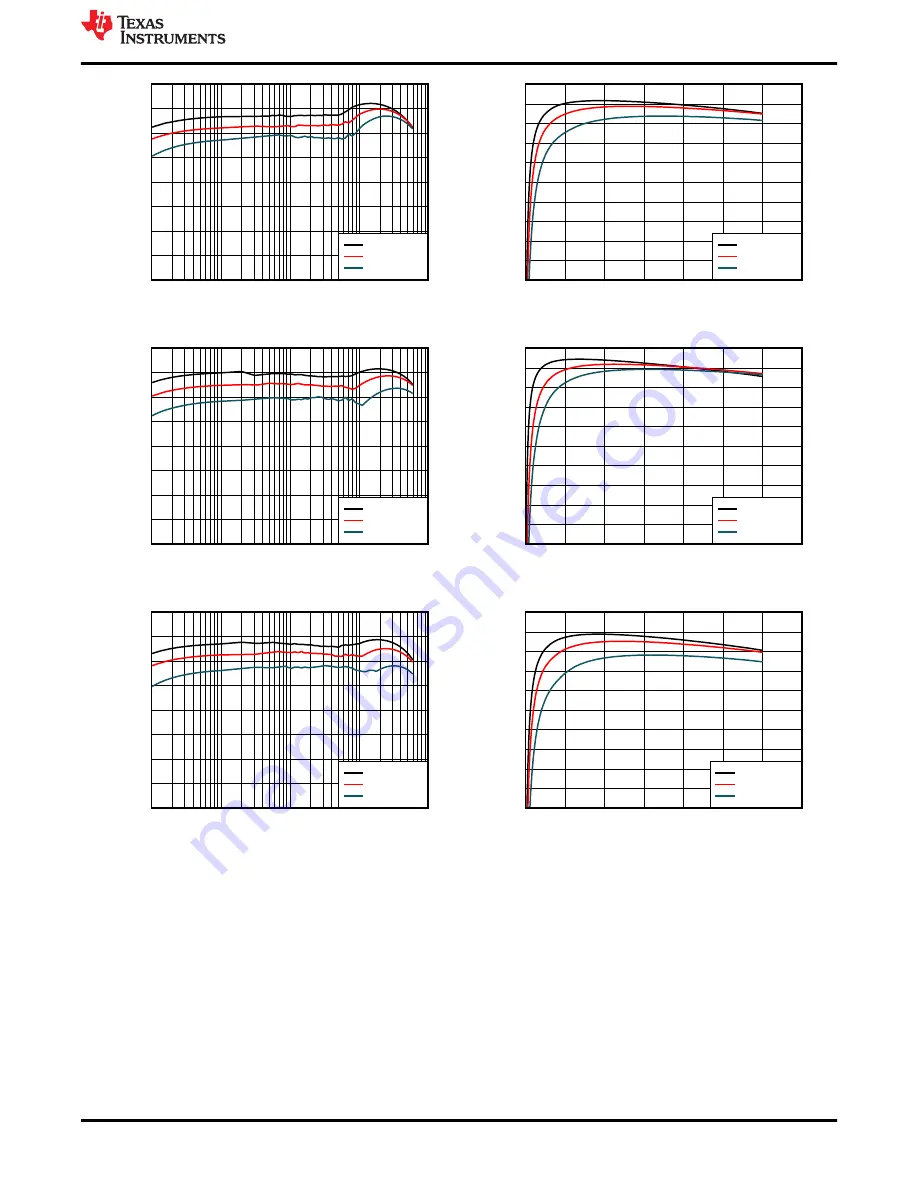
Figure 6-10. F

SW

 = 400 kHz, 3.3 VOUT, Auto Mode

Output Current (A)

Ef

fic

ie

nc

y

 (%

)

0

1

2

3

4

5

6

7

50%

55%

60%

65%

70%

75%

80%

85%

90%

95%

100%

LM61

V

IN

 = 8 V

V

IN

 = 13.5 V

V

IN

 = 24 V

Figure 6-11. F

SW

 = 400 kHz, 3.3 VOUT, FPWM Mode

Load Current (A)

Ef

fic

ie

nc

y

 (%

)

0.001

0.010.02 0.05 0.1 0.2

0.5

1

2 3 4 5 7 10

60%

65%

70%

75%

80%

85%

90%

95%

100%

LM61

V

IN

 = 8 V

V

IN

 = 13.5 V

V

IN

 = 24 V

Figure 6-12. F

SW

 = 2.2 MHz, 5 VOUT, Auto Mode

Load Current (A)

Ef

fic

ie

nc

y

 (%

)

0

1

2

3

4

5

6

7

50%

55%

60%

65%

70%

75%

80%

85%

90%

95%

100%

LM61

V

IN

 = 8 V

V

IN

 = 13.5 V

V

IN

 = 24 V

Figure 6-13. F

SW

 = 2.2 MHz, 5 VOUT, FPWM Mode

Output Current (A)

Ef

fic

ie

nc

y

 (%

)

0.001

0.010.02 0.05 0.1 0.2

0.5

1

2 3 4 5 7 10

60%

65%

70%

75%

80%

85%

90%

95%

100%

LM61

V

IN

 = 8 V

V

IN

 = 13.5 V

V

IN

 = 24 V

Figure 6-14. F

SW

 = 2.2 MHz, 3.3 VOUT, Auto Mode

Output Current (A)

Ef

fic

ie

nc

y

 (%

)

0

1

2

3

4

5

6

7

50%

55%

60%

65%

70%

75%

80%

85%

90%

95%

100%

LM61

V

IN 

 = 8 V

V

IN 

 = 13.5 V

V

IN 

 = 24 V

Figure 6-15. F

SW

 = 2.2 MHz, 3.3 VOUT, FPWM Mode

www.ti.com

LM61460EVM Board Test Results

SNVU621D – MAY 2019 – REVISED JULY 2021

Submit Document Feedback

LM61460-Q1 EVM User's Guide

15

Copyright © 2021 Texas Instruments Incorporated

Summary of Contents for LM61460EVM

Page 1: ...ent with exceptional efficiency and output accuracy in a very small solution size The EVM provides multiple power connectors and test points It also provides a good layout example which is optimized for EMI and thermal performance Table 1 1 Device and Package Configurations CONVERTER IC PACKAGE U1 LM61460 Q1 14 pin wettable flanks Hotrod package 4 0 mm 3 5 mm 1 0 mm Figure 1 1 LM61460EVM Front Fig...

Page 2: ... 6 5 Radiated EMI Measurement with Horizontal Log Antenna Under CISPR 25 Class 5 Limits 14 Figure 6 6 Radiated EMI Measurement with Vertical Log Antenna Under CISPR 25 Class 5 Limits 14 Figure 6 7 Radiated EMI Measurement with Rod Antenna Under CISPR 25 Class 5 Limits 14 Figure 6 8 FSW 400 kHz 5 VOUT Auto Mode 14 Figure 6 9 FSW 400 kHz 5 VOUT FPWM Mode 14 Figure 6 10 FSW 400 kHz 3 3 VOUT Auto Mode...

Page 3: ...emarks are the property of their respective owners www ti com Trademarks SNVU621D MAY 2019 REVISED JULY 2021 Submit Document Feedback LM61460 Q1 EVM User s Guide 3 Copyright 2021 Texas Instruments Incorporated ...

Page 4: ...omponents and has a pinout designed for optimal EMI and thermal performance Protection features include the following Thermal shutdown Input undervoltage lockout Cycle by cycle current limiting Hiccup short circuit protection The LM61460 Q1 device is pin to pin compatible with the LM61440 Q1 for easy output current scaling For a quick reference Figure 1 1 shows the pin configuration of the LM61460...

Page 5: ...current to 6 A and comes with auto mode enabled Table 1 1 EVM Variants LABEL U1 IOUT SWITCHING FREQUENCY VIN RANGE VOUT AUTO MODE FPWM SPREAD SPECTRUM LM61460EVM AS 400K LM61460AAS QRJRRQ1 6 A 400 kHz 3 to 36 V 5 V Enabled Disabled Enabled LM61460EVM FS 400K LM61460AFS QRJRRQ1 6 A 400 kHz 3 to 36 V 5 V Disabled Enabled Enabled www ti com Introduction SNVU621D MAY 2019 REVISED JULY 2021 Submit Docu...

Page 6: ...nt limit of the supply to an appropriate level to supply needed current and protection 4 Turn on the power supply With the default configuration the EVM powers up and provides VOUT 5 V 5 Monitor the output voltage with sense points The maximum load current must be 6 A with the LM61460 Q1 Note that the maximum output current may need to derate if ambient temperature is high especially if device is ...

Page 7: ...d the low ESR ceramic capacitors VIN_EMI Input voltage to input filter of the converter If the input filter is desired between the supply and the LM61460 Q1 connect the supply voltage between VIN_EMI and GND_EMI The supply voltage must be connected to the board with short and thick wires to handle pulsing input current The input filter consists of the following CF1 CF2 CF3 CF4 CF5 CF6 and L2 CD1 C...

Page 8: ... This flag is high impedance when the output voltage is in regulation Vinj To aid when making bode plots There is a low value resistor Rinj between VOUT and this node This feedback divider of the board is connected to this node as well Stimulus can be applied between this node and VOUT when taking measurements for bode plots VOUTS Kelvin sensing for VOUT This connector is provided to allow VOUT to...

Page 9: ...wer the DC DC may cause issues for ideal device operation RD2 CD2 RD1 and CD1 are placeholders for damping networks to be populated For more information regarding this topic reference the EMI Filter Components and Their Nonidealities for Automotive DC DC Regulators Technical Brief www ti com Schematic SNVU621D MAY 2019 REVISED JULY 2021 Submit Document Feedback LM61460 Q1 EVM User s Guide 9 Copyri...

Page 10: ...060 3 3 V 2100 kHz 43 2 kΩ 6 04 kΩ 3 x 22 µF 2 x 4 7 µF 2 x 100 nF 1 µH XEL5030 5 V 400 kHz 24 9 kΩ 33 2 kΩ 4 x 22 µF 2 x 4 7 µF 2 x 100 nF 4 7 µH XHMI6060 5 V 2100 kHz 24 9 kΩ 6 04 kΩ 3 x 22 µF 2 x 4 7 µF 2 x 100 nF 1 µH XEL5030 Schematic www ti com 10 LM61460 Q1 EVM User s Guide SNVU621D MAY 2019 REVISED JULY 2021 Submit Document Feedback Copyright 2021 Texas Instruments Incorporated ...

Page 11: ...here are 2 oz copper planes on the top and bottom and 1 oz copper mid layer planes to dissipate heat with an array of thermal vias to connect to all four layers Test points have been provided for ease of use to connect the power supply and required load and to monitor critical signals Figure 5 1 Top 3D View Figure 5 2 Top Layer Figure 5 3 Signal Layer 1 Ground Plane Figure 5 4 Signal Layer 2 Routi...

Page 12: ...e 5 5 Bottom Layer Figure 5 6 Bottom 3D view Board Layout www ti com 12 LM61460 Q1 EVM User s Guide SNVU621D MAY 2019 REVISED JULY 2021 Submit Document Feedback Copyright 2021 Texas Instruments Incorporated ...

Page 13: ...Hz Figure 6 2 Conducted EMI Measurement with CISPR 25 Class 5 Limit Lines 30 MHz to 110 MHz Figure 6 3 Radiated EMI Measurement with Horizontal Bicon Antenna Under CISPR 25 Class 5 Limits Figure 6 4 Radiated EMI Measurement with Vertical Bicon Antenna Under CISPR 25 Class 5 Limits www ti com LM61460EVM Board Test Results SNVU621D MAY 2019 REVISED JULY 2021 Submit Document Feedback LM61460 Q1 EVM U...

Page 14: ... mode efficiency For 2 1 MHz data the output stage has to be changed from the default BOM The inductor L1 selected was XEL5030 102MEB Load Current A Efficiency 0 0001 0 001 0 01 0 1 0 2 0 5 1 2 3 5 710 60 65 70 75 80 85 90 95 100 LM61 VIN 8 V VIN 13 5 V VIN 24 V Figure 6 8 FSW 400 kHz 5 VOUT Auto Mode Load Current A Efficiency 0 1 2 3 4 5 6 7 50 55 60 65 70 75 80 85 90 95 100 LM61 VIN 8 V VIN 13 5...

Page 15: ... 2 MHz 5 VOUT Auto Mode Load Current A Efficiency 0 1 2 3 4 5 6 7 50 55 60 65 70 75 80 85 90 95 100 LM61 VIN 8 V VIN 13 5 V VIN 24 V Figure 6 13 FSW 2 2 MHz 5 VOUT FPWM Mode Output Current A Efficiency 0 001 0 010 02 0 05 0 1 0 2 0 5 1 2 3 45 7 10 60 65 70 75 80 85 90 95 100 LM61 VIN 8 V VIN 13 5 V VIN 24 V Figure 6 14 FSW 2 2 MHz 3 3 VOUT Auto Mode Output Current A Efficiency 0 1 2 3 4 5 6 7 50 5...

Page 16: ...Mode Output Current A Output Voltage V 0 1 2 3 4 5 6 7 3 29 3 31 3 33 3 35 3 37 SNVS VIN 8 V VIN 13 5 V VIN 24 V Figure 6 18 FSW 400 kHz 3 3 VOUT Auto Mode Output Current A Output Voltage V 0 1 2 3 4 5 6 7 3 29 3 31 3 33 3 35 3 37 SNVS VIN 8 V VIN 13 5 V VIN 24 V Figure 6 19 FSW 400 kHz 3 3 VOUT FPWM Mode Output Current A Output Voltage V 0 1 2 3 4 5 6 7 4 95 4 97 4 99 5 01 5 03 5 05 5 07 5 09 5 1...

Page 17: ...T Auto Mode Output Current A Output Voltage V 0 1 2 3 4 5 6 7 3 29 3 31 3 33 3 35 3 37 SNVS VIN 8 V VIN 13 5 V VIN 24 V Figure 6 23 FSW 2 2 MHz 3 3 VOUT FPWM Mode www ti com LM61460EVM Board Test Results SNVU621D MAY 2019 REVISED JULY 2021 Submit Document Feedback LM61460 Q1 EVM User s Guide 17 Copyright 2021 Texas Instruments Incorporated ...

Page 18: ...C Q200 Grade 1 0805 0805 CGA4J3X7R1H225K125 AB TDK C21 C22 2 0 47 µF CAP CERM 0 47 µF 50 V 10 X7R AEC Q200 Grade 1 0603 0603 CGA3E3X7R1H474K080 AE TDK J1 J2 J3 3 Terminal Block 5 mm 2x1 Tin TH Terminal Block 5 mm 2x1 TH 691 101 710 002 Wurth Elektronik J4 1 Header 100 mil 3x1 Gold TH Header 100 mil 3x1 TH HTSW 103 07 G S Samtec L1 1 4 7 µH Inductor Shielded Hyperflux 4 7 µH 7 4 A 0 0143 Ω SMD 6 65...

Page 19: ...1 Automotive 6 A Low Noise Synchronous Buck Regulators RJR0014A VQFN HR 14 RJR0014A LM61460AASQRJRRQ1 LM61460EVM AS 400K or LM61460AFSQRJRRQ1 LM61460EVM FS 400K Texas Instruments C10 C11 0 22 µF CAP CERM 22 µF 16 V 20 X7R AEC Q200 Grade 1 1210 1210 CGA6P1X7R1C226M250 AC TDK C14 0 1 µF CAP CERM 1 µF 10 V 10 X7R 0603 0603 GRM188R71A105KA61D MuRata C23 C24 0 1 µF CAP CERM 1 µF 50 V 10 X7R 0603 0603 U...

Page 20: ...rmat for tables figures and cross references throughout the document 6 Added R11 to Section 7 18 Changes from Revision B November 2019 to Revision C December 2019 Page Added plots to Section 6 1 13 Added Section 6 2 14 Added Section 6 3 16 Revision History www ti com 20 LM61460 Q1 EVM User s Guide SNVU621D MAY 2019 REVISED JULY 2021 Submit Document Feedback Copyright 2021 Texas Instruments Incorpo...

Page 21: ...other than TI b the nonconformity resulted from User s design specifications or instructions for such EVMs or improper system design or c User has not paid on time Testing and other quality control techniques are used to the extent TI deems necessary TI does not test all parameters of each EVM User s claims against TI under this Section 2 are void if User fails to notify TI of any apparent defects...

Page 22: ... These limits are designed to provide reasonable protection against harmful interference in a residential installation This equipment generates uses and can radiate radio frequency energy and if not installed and used in accordance with the instructions may cause harmful interference to radio communications However there is no guarantee that interference will not occur in a particular installation...

Page 23: ...y for convenience and should be verified by User 1 Use EVMs in a shielded room or any other test facility as defined in the notification 173 issued by Ministry of Internal Affairs and Communications on March 28 2006 based on Sub section 1 1 of Article 6 of the Ministry s Rule for Enforcement of Radio Law of Japan 2 Use EVMs only after User obtains the license of Test Radio Station as provided in R...

Page 24: ... any interfaces electronic and or mechanical between the EVM and any human body are designed with suitable isolation and means to safely limit accessible leakage currents to minimize the risk of electrical shock hazard User assumes all responsibility and liability for any improper or unsafe handling or use of the EVM by User or its employees affiliates contractors or designees 4 4 User assumes all...

Page 25: ...OR DAMAGES ARE CLAIMED THE EXISTENCE OF MORE THAN ONE CLAIM SHALL NOT ENLARGE OR EXTEND THIS LIMIT 9 Return Policy Except as otherwise provided TI does not offer any refunds returns or exchanges Furthermore no return of EVM s will be accepted if the package has been opened and no return of the EVM s will be accepted if they are damaged or otherwise not in a resalable condition If User feels it has...

Page 26: ...s are subject to change without notice TI grants you permission to use these resources only for development of an application that uses the TI products described in the resource Other reproduction and display of these resources is prohibited No license is granted to any other TI intellectual property right or to any third party intellectual property right TI disclaims responsibility for and you wi...

Reviews: